A single-layer PCB, as the name suggests, consists of a single layer of conductive material with components and traces on one side.
On the other hand, multi-layer PCBs are composed of multiple layers of conductive material, sandwiched between insulating layers, with traces and components on both sides.
The choice of a single-layer or multi-layer PCB depends on various factors, including the complexity of the circuit design, cost, and performance requirements. Single-layer PCBs are relatively simple and cost-effective, making them ideal for basic electronic devices such as calculators, toys, and remote controls. They are also easy to manufacture and repair, as there is only one layer of conductive material to work with.
On the other hand, multi-layer PCBs offer several advantages over single-layer PCBs. They can accommodate complex circuit designs and provide greater flexibility in routing traces, resulting in a smaller form factor. Moreover, the additional layers of conductive material provide improved signal integrity, reducing noise and interference between components. This makes them suitable for high-performance devices such as smartphones, laptops, and servers, where signal integrity is critical.
What is Single-Layer PCB?
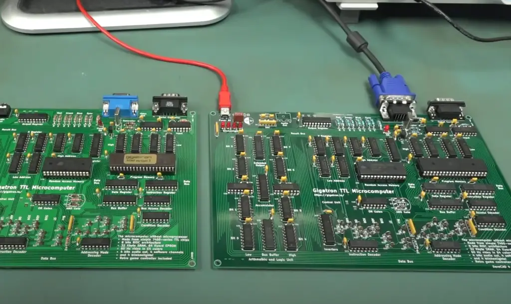
A single-layer PCB is a board made from a single sheet of material that has electrical components and conductive traces etched onto one side. This type of PCB is usually used for simple circuits in low-powered applications, such as those found in consumer electronics like computers, cell phones, and digital cameras [1].
Advantages of Single-Layer PCBs:
- Inexpensive: Single-layer PCBs are the least expensive type of PCBs. This is because they only require a single layer of copper trace, which reduces the cost of materials and manufacturing;
- Quickly Manufactured: Single-layer PCBs are easy and quick to manufacture. They require less processing and assembly time compared to other types of PCBs, which makes them ideal for prototyping and testing;
- Easy to Produce: Single-layer PCBs have a simple and straightforward design, which makes them easy to produce. They are ideal for simple circuits with few components, which makes them suitable for a wide range of applications;
- You Can Order in Bulk: Single-layer PCBs can be ordered in bulk, which makes them ideal for mass production. This can help reduce the cost of manufacturing and increase efficiency;
Disadvantages of Single-Layer PCBs:
- Limited Speed and Capacity: Single-layer PCBs have limited speed and capacity due to their simple design. They are not suitable for complex circuits with high-speed signals, which require multiple layers and more advanced design;
- It Does Not Offer Much Space: Single-layer PCBs have limited space for components due to their simple design. They are not suitable for circuits with many components or large-sized components;
- Larger and Heavier: Single-layer PCBs are larger and heavier compared to other types of PCBs due to their simple design. This can make them unsuitable for applications where size and weight are critical;
Applications of Single-Layer PCBs
- Consumer Electronics: Single-layer PCBs are commonly used in consumer electronics, such as televisions, radios, and calculators. They are ideal for simple circuits with few components, which makes them suitable for low-cost products;
- Automotive Industry: Single-layer PCBs are also used in the automotive industry for applications such as dashboard controls and sensors. They are suitable for low-power and low-speed circuits, which makes them ideal for these applications;
- Industrial Automation: Single-layer PCBs are used in industrial automation for applications such as control systems and sensors. They are suitable for low-speed and low-power circuits, which makes them ideal for these applications;
- Medical Devices: Single-layer PCBs are also used in medical devices for applications such as patient monitoring and diagnostic equipment. They are suitable for low-power and low-speed circuits, which makes them ideal for these applications;
What is Multi-Layer PCB?
Multi-layer PCBs are boards with multiple layers, each containing electrical components and conductive traces. The number of layers can range anywhere from two to eight or more. Multiple layers allow the circuit to be much more complex than it would be on a single-layer board and enable higher-power applications such as automotive systems or industrial robots [2].
Advantages of Multi-Layer PCBs
- Complex Projects: Multi-layer PCBs are ideal for complex projects that require multiple circuits or components. The multiple layers provide more space for components and allow for more complex designs, which makes them suitable for high-performance devices;
- More Durable: Multi-layer PCBs are more durable than single-layer PCBs because they can withstand more stress and strain. The multiple layers provide additional support, which makes them more resistant to vibration, heat, and other environmental factors;
- Connection: Multi-layer PCBs offer better connections between components due to their multiple layers of copper trace. This allows for more efficient transfer of signals and reduces the risk of interference or noise;
- More Power: Multi-layer PCBs can handle more power compared to single-layer PCBs. This is because they have multiple layers of copper trace, which allows for a more efficient transfer of power between components;
Disadvantages of Multi-Layer PCBs:
- More Expensive: Multi-layer PCBs are more expensive than single-layer PCBs due to their complexity and the additional layers of copper trace. This can make them unsuitable for low-cost products or projects with limited budgets;
- Lengthy Lead Time: The manufacturing process for multi-layer PCBs is more complex and time-consuming than for single-layer PCBs. This can result in longer lead times for production and delivery, which can be a disadvantage for time-sensitive projects;
- Repairs Can be Complex: Multi-layer PCBs can be more challenging to repair than single-layer PCBs. This is because the additional layers of the copper trace can make it difficult to locate and fix the source of the problem;
Applications of Multi-Layer PCBs:
- Telecommunications: Multi-layer PCBs are commonly used in telecommunications equipment, such as cell phones, routers, and modems. They are suitable for high-performance circuits that require efficient signal transfer and power handling;
- Computer Hardware: Multi-layer PCBs are also used in computer hardware, such as motherboards and graphics cards. They are suitable for high-performance circuits that require efficient signal transfer and power handling;
- Medical Equipment: Multi-layer PCBs are used in medical equipment, such as ultrasound machines and MRI scanners. They are suitable for high-performance circuits that require efficient signal transfer and power handling;
- Aerospace and Defense: Multi-layer PCBs are used in aerospace and defense applications, such as guidance systems and radar equipment. They are suitable for high-performance circuits that require efficient signal transfer and power handling in extreme environments;

Differences – Single Layer PCB Vs Multi-Layer PCB
1) Manufacturing Process
Single-layer PCBs have a relatively simple manufacturing process compared to multi-layer PCBs. The process involves printing a layer of conductive material, usually copper, onto a non-conductive substrate, such as fiberglass or plastic. The next step is to etch away the excess copper using a chemical solution to create the desired circuit pattern. Finally, the board is drilled to create holes for component leads and other connections.
On the other hand, multi-layer PCBs have a more complex manufacturing process. The process involves stacking multiple layers of copper and non-conductive substrate, which are then bonded together with a special adhesive. The layers are then etched to create the desired circuit patterns, and the board is drilled to create holes for component leads and other connections. The multiple layers of copper and substrate can create a more complex circuit design and allow for more components to be included on the board [3].
2) Material
The materials used in single-layer PCBs and multi-layer PCBs also differ. Single-layer PCBs are usually made from a non-conductive substrate, such as fiberglass or plastic, with a layer of conductive material, such as copper, on one side. The thickness of the copper layer can vary depending on the requirements of the circuit design.
Multi-layer PCBs are made from multiple layers of conductive material and non-conductive substrate, which are bonded together with a special adhesive. The number of layers can vary depending on the requirements of the circuit design. The materials used in multi-layer PCBs are typically more expensive than those used in single-layer PCBs due to the additional layers and complexity of the manufacturing process.
3) Cost
Single-layer PCBs are generally less expensive than multi-layer PCBs due to their simpler manufacturing process and lower material costs. Single-layer PCBs are suitable for low-cost products or projects with limited budgets. However, single-layer PCBs have limitations in terms of complexity, speed, and power handling.
Multi-layer PCBs are suitable for high-performance devices that require efficient signal transfer and power handling. The additional layers and complexity allow for more components to be included on the board, which can reduce the size of the device and improve its performance.
4) Application
Single-layer PCBs are suitable for simple electronic devices that require a basic circuit design, such as toys, calculators, and remote controls.
Multi-layer PCBs are suitable for complex electronic devices that require a more complex circuit design, such as smartphones, computers, and medical equipment. They are also suitable for high-performance devices that require efficient signal transfer and power handling. The additional layers and complexity allow for more components to be included on the board, which can reduce the size of the device and improve its performance [4].
Single-Side vs Double-Side PBCs
Single-side PCBs are constructed with a single layer of wiring and components on one side of the board. These boards are typically used in simpler electronic designs, as putting all of the components and wiring on one side simplifies the design process. Single-side PCBs also tend to be less expensive than other types, since they require fewer layers and materials to produce.
Double-sided PCBs, on the other hand, feature two conductive layers separated by an insulating material. This type of board is more complex but offers more flexibility in terms of component placement and routing capabilities. Double-sided boards can also support larger parts, allowing for a higher level of integration in a given design. They are also more expensive to produce than single-sided boards, due to the additional layers and materials needed for fabrication [5].
How to Identify a Multi-Layer PCB?
Multi-layer PCBs are easily identified by their physical characteristics:
- The PCB will appear thicker than a single-layer board, due to the additional layers of copper and other materials used in its construction;
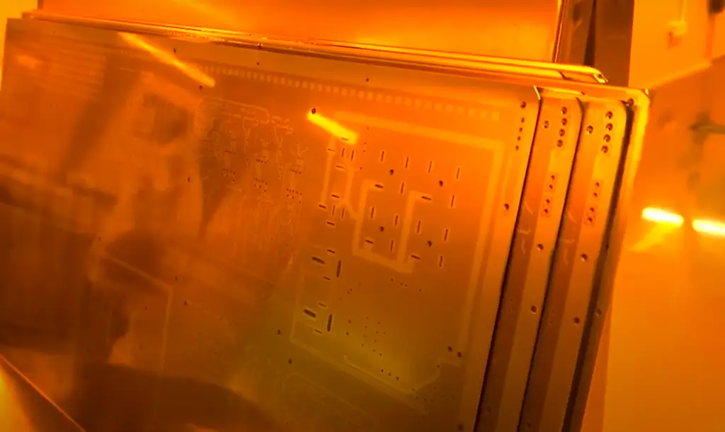
- Additionally, when looking at a multi-layer board from the top or bottom view, you can see radiating lines or circles on either side of the through-hole components. This is a clear indicator that multiple layers have been used in its construction. When held up to the light, each layer of the PCB is visible as well;
- Lastly, although they are often more expensive to produce than single-layer boards, multi-layer boards offer much greater complexity and functionality for larger projects. As such, they are becoming increasingly popular for use in today’s electronics and technology;
Deciding Whether You Need Single-Layer or Multi-Layer PCBs:
What Level Of Functionality Do I Need?
One of the first considerations when deciding whether to use a single-layer or multi-layer PCB is the level of functionality required. Single-layer PCBs are simpler in design and have only one layer of conductive material on the board’s surface. They are ideal for basic applications that require only a few components, such as simple sensors, timers, or switches.
Multi-layer PCBs, on the other hand, are more complex and have multiple layers of conductive material stacked on top of each other. This makes them suitable for more advanced applications that require more complex circuits, such as microprocessors or high-frequency communication devices.
Therefore, if you need to create a device with more advanced functionality, you will likely require a multi-layer PCB. However, if your application requires only basic functionality, a single-layer PCB may suffice [6].
What Is The Maximum Size The Board Can Be?
Another consideration is the maximum size the board can be. Single-layer PCBs are ideal for small to medium-sized boards, while multi-layer PCBs can accommodate larger designs. This is because single-layer PCBs have limited space for components and circuit traces.
If your application requires a larger board, you will likely need a multi-layer PCB. However, if your device requires only a small to medium-sized board, a single-layer PCB may be more suitable.
Is Durability A Priority?
The durability of the PCB is another factor to consider.
The conductive material on a single-layer PCB is prone to damage from environmental factors such as moisture and heat.
Multi-layer PCBs are more durable and can withstand more wear and tear. They are also less susceptible to environmental factors, making them ideal for applications that require long-term reliability.
Therefore, if durability is a priority for your application, you should consider a multi-layer PCB. However, if your device is not exposed to harsh environmental conditions, a single-layer PCB may be sufficient.
What Is My Budget?
Finally, your budget is an important consideration when deciding whether to use a single-layer or multi-layer PCB. Single-layer PCBs are less expensive to produce than multi-layer PCBs because they are less complex in design.
Multi-layer PCBs require more materials, more intricate manufacturing processes, and more testing, which makes them more expensive. Therefore, if your budget is limited, a single-layer PCB may be the more economical option.
Nevertheless, it is important to note that the cost of a PCB can vary depending on the supplier and other factors such as the quantity ordered. Therefore, it is always a good idea to shop around and compare prices from different suppliers before making a final decision [7].
How Quickly Do I Need the PCBs?
The timeline for PCB production can vary depending on several factors such as the complexity of the design, the number of layers required, and the manufacturing process used. Typically, single-layer PCBs can be produced faster than multi-layer PCBs due to their simpler manufacturing process. However, the lead time for both types of PCBs can vary depending on the manufacturer and the quantity ordered.
If you have a tight deadline for your project and need the PCBs quickly, you can discuss the timeline with the manufacturer or supplier. Some manufacturers offer expedited production and shipping services for an additional fee. However, it is important to note that rushing the production process can increase the risk of errors and may impact the quality of the final product.
It is recommended to plan ahead and allow enough time for the PCB production and testing process. This can help ensure that the PCBs are produced correctly and meet the required specifications. It is also a good practice to order a few extra PCBs to account for any potential defects or issues that may arise during the manufacturing process.

FAQ
1. What does it mean if a PCB has multiple layers?
A PCB with multiple layers means that it has more than one layer of conductive material sandwiched between insulating layers. Multi-layer PCBs are used in electronic devices that require more complex circuit designs, as they provide greater flexibility in routing traces and accommodating more components.
2. What are single-layer PCBs used for?
Single-layer PCBs are used in basic electronic devices that require simple circuit designs, such as calculators, toys, and remote controls. They are relatively simple and cost-effective to manufacture and repair, making them ideal for low-cost applications [8].
3. What is the advantage of more than one layer of PCB?
The advantage of more than one layer of PCB is that it can accommodate complex circuit designs and provide greater flexibility in routing traces, resulting in a smaller form factor. Moreover, the additional layers of conductive material provide improved signal integrity, reducing noise and interference between components, making them suitable for high-performance devices where signal integrity is critical.
4. What is an example of a multi-layer PCB?
An example of a multi-layer PCB is a smartphone motherboard, which contains several layers of conductive material and insulating layers to accommodate the complex circuit design and miniaturize the form factor.
5. What material is used for multilayer PCB?
Multilayer PCBs are typically made of a combination of materials, including copper, FR-4 epoxy, and polyimide. Copper is used for the conductive layers, while FR-4 epoxy and polyimide are used for the insulating layers [9].
6. Do I need a 4-layer PCB?
The need for a 4-layer PCB depends on the complexity of the circuit design and the performance requirements of the electronic device. A 4-layer PCB is typically used for devices that require more complex circuit designs and better signal integrity than what a single-layer or 2-layer PCB can offer [10].
7. What is a 7-layer PCB?
They are typically used in high-performance electronic devices such as servers, where signal integrity and circuit density are critical.
8. What is a 2-layer PCB vs a 4-layer PCB?
A 2-layer PCB has two layers of conductive material and insulating layers, while a 4-layer PCB has four layers of conductive material and insulating layers. The main advantage of a 4-layer PCB is that it can accommodate more complex circuit designs and provide better signal integrity than a 2-layer PCB [11].
9. How thick is a multi-layer PCB?
The thickness of a multilayer PCB depends on the number of layers, the thickness of the conductive and insulating layers, and the overall size of the PCB. Typically, multilayer PCBs can range from 0.4mm to 3.2mm in thickness [12].
10. How do I choose a PCB layer?
The choice of PCB layer depends on the complexity of the circuit design, the performance requirements of the electronic device, and the cost constraints. A single-layer PCB is suitable for simple circuit designs, while a multi-layer PCB is suitable for complex circuit designs that require better signal integrity and miniaturization.
11. What is the most layers in a PCB?
The number of layers in a PCB can vary, but the highest number of layers recorded in commercial use is 140 layers. However, such high-layer count PCBs are rare and expensive, and most commercial PCBs have a layer count ranging from 2 to 16 layers [13].
12. How thick is 1 layer PCB?
The thickness of a 1-layer PCB depends on the type of substrate used and the copper weight. Generally, the thickness of a standard FR4 PCB substrate is around 1.6mm, and the thickness of the copper layer ranges from 1oz to 4oz. Therefore, the total thickness of a 1-layer PCB can range from 1.6mm to 2.4mm [14].
13. Are all PCBs the same?
No, not all PCBs are the same. PCBs can differ in terms of the number of layers, materials used, thickness, size, and complexity of the circuit design. PCBs can be customized to suit specific requirements and applications, and their properties can be tailored to meet the desired performance criteria.
14. What are the 3 methods of PCB designing?
Schematic capture involves creating a circuit diagram, PCB layout involves designing the physical layout of the circuit on the board, and PCB fabrication involves manufacturing the board according to the design specifications.
15. What are the advantages of multilayer coating?
The advantages of multilayer coating include improved resistance to environmental factors such as heat, moisture, and chemical exposure, improved electrical performance, better signal integrity, and enhanced reliability.
16. Is black PCB better than green?
The color of the PCB has no effect on its performance. The choice of PCB color is primarily an aesthetic preference, and different colors are used to distinguish between different PCBs or signal layers.
17. What is the difference between PCB boards?
The difference between PCB boards can lie in the number of layers, the materials used, the thickness, the size, and the complexity of the circuit design. PCB boards can be customized to meet specific requirements and applications, and the properties of the PCB can be tailored to achieve the desired performance.
18. How many PCBs are in a panel?
The number of PCBs in a panel depends on the size of the board and the manufacturer’s capabilities. Panels can range from a single board to several hundred boards, depending on the size and shape of the board.
19. Why is double-sided PCB more expensive?
Double-sided PCBs are more expensive than single-layer PCBs because they require more materials and more complex manufacturing processes. Double-sided PCBs have more components, require more drilling and plating, and need to be laminated and etched on both sides, which increases the cost of manufacturing.
20. How thick is 20-layer PCB?
The thickness of a 20-layer PCB depends on the materials used and the manufacturer’s capabilities. Generally, a 20-layer PCB can have a thickness ranging from 1.6mm to 4mm [15].
21. What is the difference between type 3 and type 4 PCB?
Type 3 and type 4 PCBs are classification standards defined by the Institute of Printed Circuits (IPC). Type 3 PCBs are used for complex circuit designs that require high-density interconnections and have a layer count of up to 10 layers. Type 4 PCBs are used for more complex circuit designs that require higher layer counts, with a maximum layer count of 28 layers.
Type 4 PCBs have tighter tolerances and higher reliability requirements than Type 3 PCBs and are used for applications such as aerospace, military, and medical devices. The main difference between Type 3 and Type 4 PCBs is the number of layers and the performance requirements [16].
Useful Video: DIFFRENCE BETWEEN SINGLE LAYER AND DOUBLE LAYER PCB
References
- https://www.pcbcart.com/article/content/single-layer-vs-multi-layer-pcbs.html
- https://www.electronicsandyou.com/single-layer-pcb-vs-multi-layer-pcb.html
- https://www.911eda.com/articles/single-layer-vs-multilayer-pcbs-how-do-they-differ
- https://resources.pcb.cadence.com/blog/2022-comparing-single-sided-pcbs-vs-double-sided-pcbs
- https://aapcb.com/new-blog/single-layer-vs-multi-layer-pcbs-differences-explained/
- https://www.pcbgogo.com/Blog/Single_Sided_vs__Double_Sided_vs__Multilayer_PCBs.html
- https://wellerpcb.com/the-difference-single-layer-2-layer-and-multi-layer-printed-circuit-boards/
- https://www.ymspcb.com/news/single-layer-vs-multilayer-pcbs-how-do-they-differ
- https://www.mclpcb.com/blog/single-double-vs-multilayer/
- https://indiacircuit.com/single-layer-vs-multi-layer-pcb/
- https://www.unitepcb.com/the-difference-between-single-layer-and-multi-layer-pcb
- https://www.pcbtrain.co.uk/blog/single-layer-vs-multi-layer-pcbs
- https://suntronicinc.com/blog/know-the-difference-between-single-layer-and-multilayer-pcbs/
- https://www.avanticircuits.com/single-and-multilayer-pcbs-know-the-difference/
- https://www.exceptionpcb.com/whats-the-difference-between-single-and-double-sided-printed-circuit-boards/
- https://www.tcadian.com/2023/02/the-difference-between-single-layer-pcb.html




Leave a Reply