PCBs are used in a vast range of applications, including computers, smartphones, medical devices, automobiles, and many other electronic devices. However, as the complexity and sophistication of electronic devices have increased, so too have the demands placed on PCBs.
PCBs are required to perform reliably, efficiently, and error-free in a range of challenging environments. Any defects or malfunctions in PCBs can lead to serious consequences, ranging from decreased product quality to equipment failure, safety hazards, and costly recalls. To ensure the performance, reliability, and safety of PCBs, functional testing is an essential step in the manufacturing process.
In this article, we will explore the importance of PCB functional testing services, the types of tests that are commonly performed, and the benefits of working with a reliable and experienced PCB functional testing service provider.
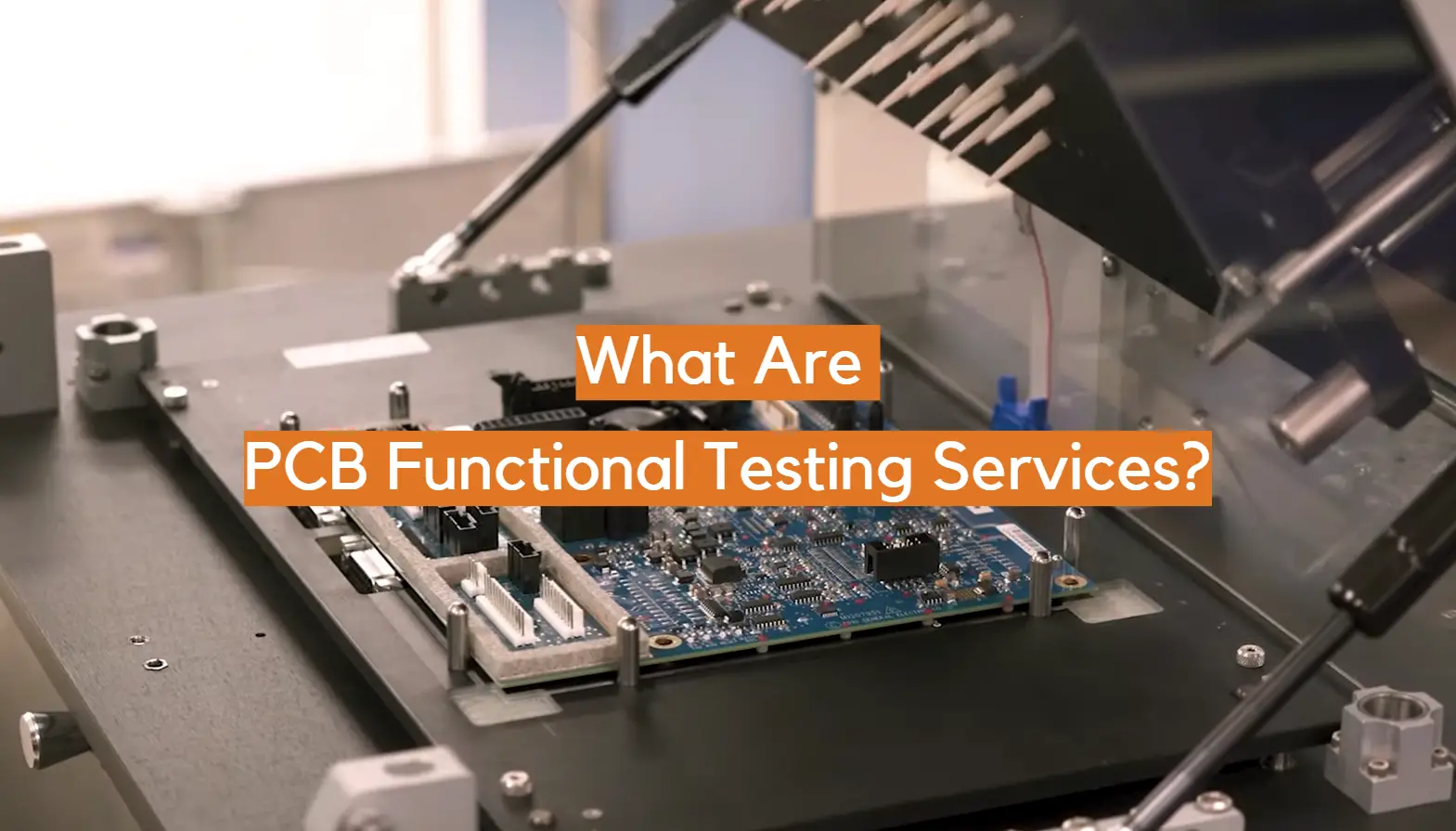
What is PCB Functional Testing?
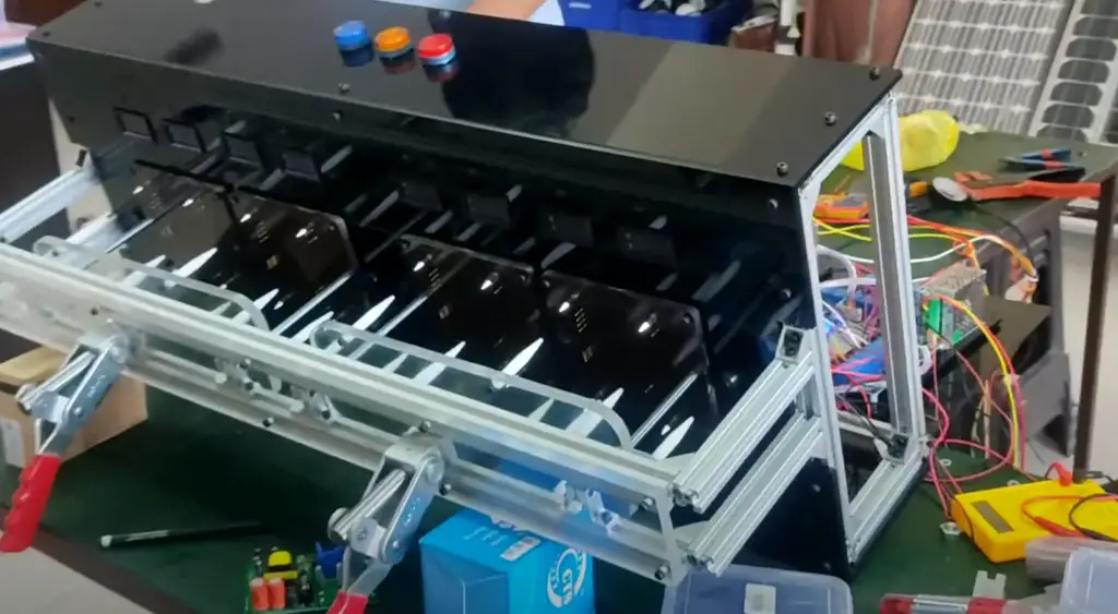
PCB functional testing services involve testing the electrical and mechanical properties of a PCB to ensure that it meets the desired specifications and performs correctly in its intended application. Functional testing can be performed at different stages of the manufacturing process, including pre-production testing, in-circuit testing, and final testing [1].
Pre-production testing is performed to verify the design and functionality of a PCB before it is mass-produced. In-circuit testing is conducted on individual PCBs during production to ensure that each board meets the desired specifications.
Final testing involves testing the completed product to ensure that it meets the intended performance requirements. Functional testing can also be performed in various environments, including temperature and humidity chambers, vibration and shock chambers, and electromagnetic interference (EMI) chambers, to simulate real-world conditions that the PCB may encounter.
PCBA Functional Testing In Details:
Voltage & Power
Voltage and power are crucial aspects of PCBA functional testing. The PCBA must be able to deliver the required voltage and power to all the components for them to function correctly. A power supply unit (PSU) is used to test the voltage and power delivery capabilities of the PCBA. The PSU is used to simulate different voltage and power requirements and test if the PCBA can deliver the required voltage and power to all the components.
In addition to testing the voltage and power delivery capabilities of the PCBA, the PSU can also be used to test the power consumption of the PCBA. The power consumption of the PCBA should be within the expected range, and any deviation from the expected range can indicate a defect or malfunction.
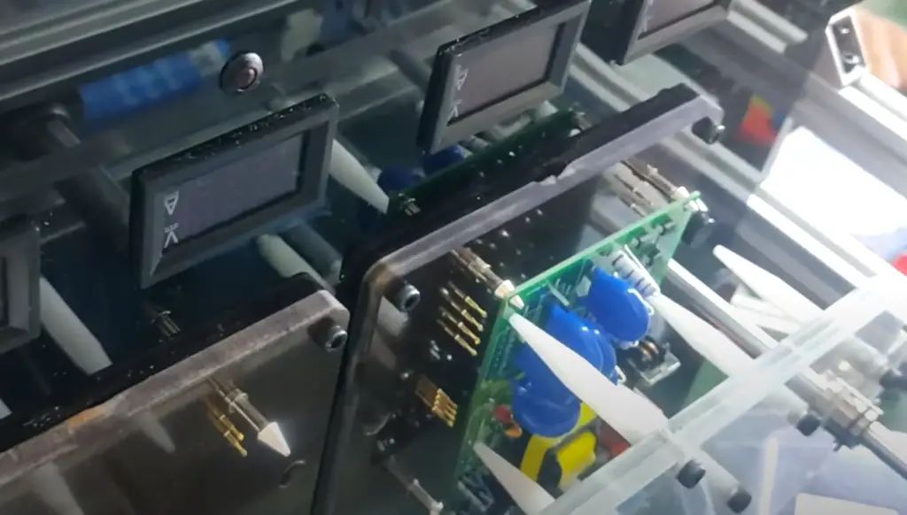
Microcontrollers & Processors
Microcontrollers and processors are critical components of the PCBA. They are responsible for the device’s overall functionality and must be tested to ensure that they are functioning correctly. The testing of microcontrollers and processors involves testing their performance under different conditions.
For example, the microcontroller’s response time can be tested by simulating different inputs and checking the response time. The processor’s performance can be tested by running various software programs and checking the response time and overall performance [2].
In addition to testing the performance of microcontrollers and processors, it is also essential to test their compatibility with other components on the PCBA. This involves testing the communication protocols between the microcontrollers/processors and other components, such as sensors or user interfaces.
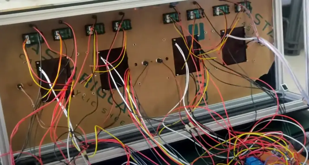
Signals & Sensors
Signals refer to the electrical signals that are transmitted between different components on the PCBA. Sensors, on the other hand, are electronic components that detect physical changes, such as temperature, pressure, or motion.
Testing signals and sensors involve checking the accuracy and reliability of the signals and sensors. For example, the accuracy of a temperature sensor can be tested by exposing it to different temperatures and checking if the readings are within the expected range. The reliability of a signal can be tested by simulating different input scenarios and checking if the output signal is within the expected range.
User Interfaces
Testing user interfaces involves checking the responsiveness and accuracy of the input and output mechanisms.
For example, the responsiveness of a button can be tested by measuring the time between the button press and the response. The accuracy of a touchscreen can be tested by simulating different touch scenarios and checking if the input is accurate and reliable.
In addition to testing the responsiveness and accuracy of user interfaces, it is also essential to test their compatibility with other components on the PCBA. This involves testing the communication protocols between the user interfaces and other components, such as microcontrollers or processors.
Why PCB Functional Testing Is Crucial and How Does It Matter to You?
When it comes to creating a PCB (Printed Circuit Board), functional testing is an essential part of the process. This type of testing ensures that the printed circuit board meets specific requirements and specifications, as well as performs reliably in its environment.
Functional tests can take many forms, depending on the application for which it’s being designed. Testing might include power-on/power-off testing, checking for correct component operation at various temperatures, or even connecting with other devices and checking communication protocols. The goal of these tests is to make sure the product meets user requirements before releasing it into the market.
PCB Functional Testing Capabilities:
- Power-On/Power-Off Testing;
- Temperature Tests of Components;
- Component Functional Tests;
- Connectivity and Protocol Checks;
- System Level Testing;
- Environmental Stress Testing;
Benefits of PCB Functional Testing Service:
- Improved Quality: Functional testing helps to ensure that the product meets all of the user requirements;
- Increased Reliability: Through thorough testing, it’s possible to identify any potential design problems and make changes before going into production. This minimizes the risk of errors or malfunction when in use;
- Reduced Costs: By taking proactive measures and identifying issues ahead of time, you can save costs by reducing rework and avoiding returns or warranty claims due to faulty products;
- Faster Time To Market: With functional testing services, you can reduce development time and speed up your product launch timeline [3];
Application of PCB Functional Testing
PCB functional testing services are used in a variety of applications, including automotive, aerospace, medical devices, and consumer electronics. Depending on the application, these tests may be performed in-house or outsourced to an experienced contract manufacturer.
Common PCB Functional Testing Techniques:
Test Procedure List Creation
Test procedure list creation is an essential step in PCB functional testing. The test procedure list outlines the various tests that need to be performed on the PCB to ensure that it is functioning correctly. The list typically includes tests for voltage and current, load testing, signal testing, and other specific tests that are required for the particular PCB being tested.
Creating a test procedure list involves analyzing the PCB’s design, identifying potential problem areas, and determining the appropriate tests to be performed. Once the list is created, it serves as a guide for the testing process, ensuring that all necessary tests are performed.
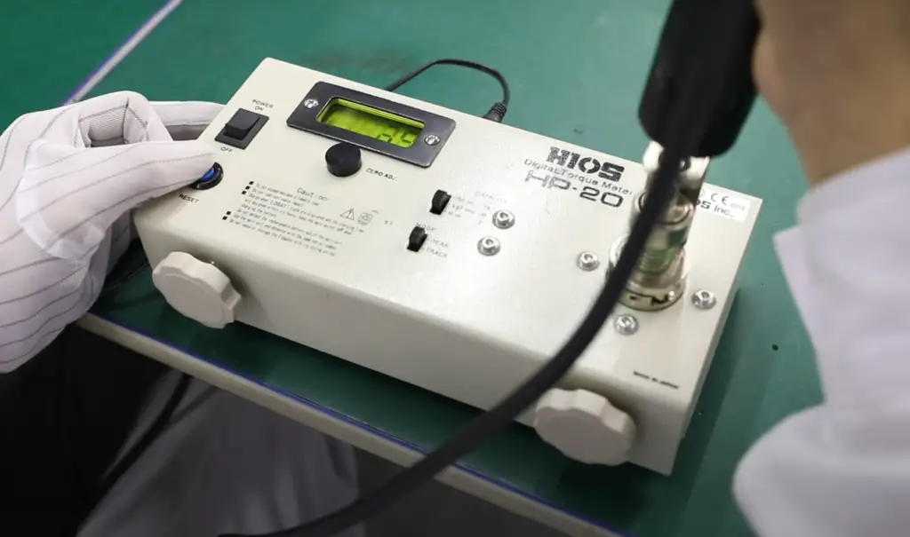
Voltage Meter Testing
Voltage meter testing is a commonly used technique in PCB functional testing. This technique involves measuring the voltage across different points on the PCB to ensure that the voltage is within the expected range. A voltage meter is used to measure the voltage, and the results are compared to the expected values.
Voltage meter testing is typically performed at different stages of the manufacturing process, including after the soldering process and before the final assembly. This technique can help identify problems such as voltage drops, which can indicate a problem with the power delivery system on the PCB [4].
Load Testing
Load testing is another commonly used technique in PCB functional testing. This technique involves subjecting the PCB to various loads to ensure that it can handle the expected workload. The load testing can be performed using specialized equipment, such as load banks or resistive loads, which simulate the expected load on the PCB.
Load testing is typically performed after the voltage meter testing to ensure that the PCB can deliver the required voltage and power to the components under the expected load. This technique can help identify problems such as overheating or power consumption issues, which can affect the overall performance of the PCB.
QC Testing
Quality control (QC) testing is a comprehensive testing technique that covers all aspects of the PCB’s functionality. QC testing involves performing a series of tests that verify the PCB’s performance, including voltage and current testing, load testing, signal testing, and other specific tests as required.
QC testing is typically performed before the PCB is assembled into the final product to ensure that it meets the required quality standards. This technique can help identify problems such as component defects, incorrect assembly, or other issues that can affect the PCB’s performance.
How PCB Functional Testing Works:
PCB X-ray Inspection Service
PCB X-ray inspection services are a valuable tool in PCB functional testing. This technique involves using X-ray technology to inspect the internal components of the PCB. X-ray inspection can detect hidden defects such as broken or cracked components, solder voids, and missing components that may not be visible during visual inspection.
PCB X-ray inspection is typically performed after the soldering process and before the final assembly. This technique can help identify potential problems early in the manufacturing process, reducing the overall cost of manufacturing and ensuring that the final product is of high quality.
Micro-Sectioning Analysis
Micro-sectioning analysis can detect problems such as incorrect soldering, voids, delamination, and other defects that may affect the overall performance of the PCB.
The micro-sectioning analysis is typically performed after the soldering process and before the final assembly. This technique can help identify potential problems early in the manufacturing process, reducing the overall cost of manufacturing and ensuring that the final product is of high quality [5].
PCB Contamination Tests
PCB contamination tests are essential in PCB functional testing. This technique involves testing the PCB for contaminants that may affect its performance. Contaminants can include dirt, dust, grease, and other substances that may have accumulated on the PCB during the manufacturing process.
PCB contamination tests are typically performed after the soldering process and before the final assembly. This technique can help identify potential problems early in the manufacturing process, reducing the overall cost of manufacturing and ensuring that the final product is of high quality.
PCB Solderability Testing
Solderability testing can identify problems such as insufficient solder, cold solder joints, and other defects that may affect the overall performance of the PCB.
PCB solderability testing is typically performed after the soldering process and before the final assembly. This technique can help identify potential problems early in the manufacturing process, reducing the overall cost of manufacturing and ensuring that the final product is of high quality.
Time-Domain Reflectometer Test (TDR)
The Time-Domain Reflectometer Test (TDR) is a valuable tool in PCB functional testing. This technique involves sending a signal down a trace on the PCB and measuring the reflection of the signal. TDR can identify problems such as impedance mismatches, open circuits, and other defects that may affect the overall performance of the PCB.
TDR is typically performed after the PCB is assembled into the final product. This technique can help identify potential problems early in the manufacturing process, reducing the overall cost of manufacturing and ensuring that the final product is of high quality [6].
Peel Test
The peel test is another valuable tool in PCB functional testing. This technique involves applying force to a component on the PCB and measuring the force required to remove the component from the PCB. The peel test can identify problems such as insufficient adhesive or poor bonding between the component and the PCB.
The peel test is typically performed after the PCB is assembled into the final product. This technique can help identify potential problems early in the manufacturing process, reducing the overall cost of manufacturing and ensuring that the final product is of high quality.
PCB Solder Float Test
The PCB solder float test is a valuable tool in PCB functional testing. This technique involves placing the PCB in a molten solder bath and measuring the time it takes for the PCB to float to the surface. The PCB solder float test can identify problems such as insufficient solder or poor bonding between the PCB and the components.
The PCB solder float test is typically performed after the soldering process and before the final assembly. This technique can help identify potential problems early in the manufacturing process, reducing the overall cost of manufacturing and ensuring that the final product is of high quality.
How to Test:
Functional Test Plan
Functional testing service involves creating a test plan to ensure that all components of the printed circuit board (PCB) are working according to the desired specifications. The functional test plan should include pre-defined criteria for each component, including pass/fail criteria for all tests performed. To perform the functional test, technicians use a combination of automated tests and manual inspections to verify whether or not the PCB meets its intended functionality requirements.
Automated tests may include measurements of current draw, power supply voltages, signal levels, and continuity checks. Manual inspections might involve visual inspection of solder joints, checking mechanical assembly performance, and observing device behavior during normal operation. Once all tests have been completed successfully, it is time to create a report summarizing the results of the testing [7].
The report should include a detailed description of any failures that occurred during the test, along with corrective action steps necessary to resolve the failure. A summary of all tests performed and any noted discrepancies should also be included in the report. This data can then be used by engineers to determine if adjustments are needed or whether further testing or troubleshooting is required. A functional test plan helps ensure that the PCB meets its intended purpose and performs as expected for its lifetime.
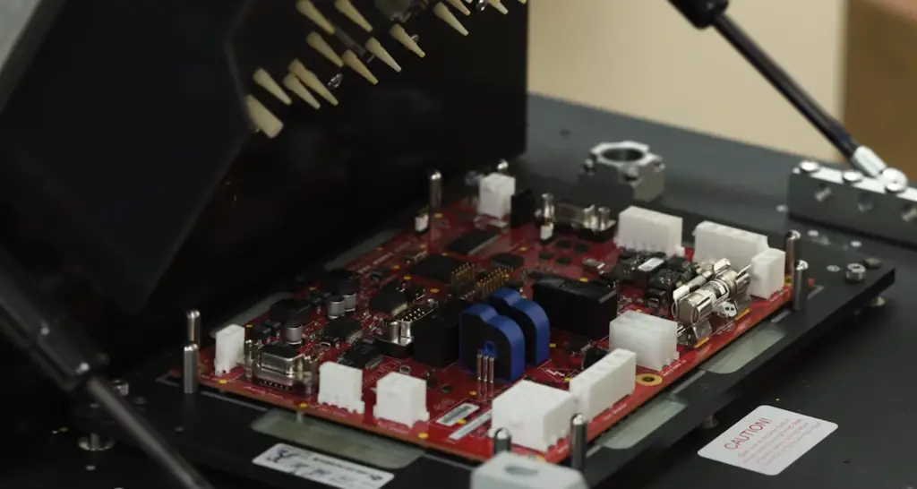
Test Points
When developing a functional test plan, it is important to include test points that will be used to verify that all components of the PCB are working correctly. These test points should include measurements of current draw, power supply voltages, signal levels, and continuity checks. For automated tests, the exact parameters for each of these tests should be defined in advance. This helps ensure consistent results by providing technicians with specific criteria that must be met before they can pass or fail any component.
The number of test points necessary will depend on the complexity of the PCB design and its intended purpose. Generally speaking, more complex designs will require more test points than simpler ones. Once all testing has been completed successfully and final results have been reported, engineers typically use this data to make adjustments to their design if necessary.
In-System Programming
This technique involves connecting an in-circuit programmer directly to the IC device, which then reads and modifies stored information in internal memory [8].
ISP can be used to test components such as microcontrollers, memories, digital signal processors, and other programmable logic devices. This process helps engineers verify that their design works as expected before turning it into a finished product. Additionally, ISP can also be used to diagnose problems with existing PCBs and make necessary corrections or adjustments quickly and easily.
Common PCB Assembly Issues
Functional testing of printed circuit boards (PCBs) is an essential part of the manufacturing process, as it ensures that all components are functioning correctly and that there are no errors or defects in the assembly. However, even with functional testing, there may be common PCB assembly issues that require further inspection and corrective action.
Below is a list of some common issues that arise during PCB functional testing:
- Short circuits: Short circuits occur when two different conductors touch each other due to improper insulation or faulty wiring. This can lead to faulty operation and/or complete failure of the device;
- Open circuits: An open circuit occurs when a wire breaks during soldering, which leads to an interruption in the electrical current. This issue can be difficult to diagnose and repair, so it is important for PCB manufacturers to use reliable soldering techniques;
- Heat damage: Excessive heat during soldering can cause components on the board to become damaged or burned out. To avoid this issue, it’s important to ensure that components are not exposed to too much heat during assembly;
- Poor connections: Poor wiring connections can lead to poor conductivity between two points, leading to a decrease in the performance of the device. It’s important for manufacturers to properly inspect each connection before and after assembly [9];
What Can’t PCB Functional Testing Do?
PCB functional testing cannot detect some issues, such as a weak connection or poor soldering. These types of problems require visual inspection and rework. PCB functional testing can also be time-consuming, requiring multiple test runs to make sure all parts are functioning properly.
Additionally, if there are hidden design flaws in the board that do not appear until the end of the production cycle, then these will not be detected until later in the process. For this reason, it is important for designers to thoroughly consider their designs before beginning production and testing.
Lastly, some components used on a PCB may have difficulty being tested with automated methods and require manual procedures instead. This means more work for testers who must be able to identify which components need additional testing.
PCB functional testing still offers invaluable services, but it is not a complete solution for identifying every potential issue with a board. It should be used in conjunction with other methods such as visual inspection and rework to ensure the highest quality boards are produced. With proper utilization of these techniques, manufacturers can produce reliable and functioning products with fewer defects.
How To Choose PCB Functional Testing Services:
Well-Equipped Testing Facility
One of the most critical factors to consider when choosing PCB functional testing services is the testing facility’s equipment. The testing facility should have state-of-the-art equipment to ensure accurate and reliable testing results. The testing equipment should also be well-maintained and calibrated to provide consistent and repeatable results.
Some of the critical testing equipment that a PCB functional testing facility should have includes:
- Oscilloscopes are used to measure the electrical signals on the PCB. They are used to determine if the signals are within the expected range and if there are any abnormalities or inconsistencies;
- Logic analyzers are used to analyze digital signals on the PCB. They are used to check the timing and synchronization of digital signals and to detect any errors or glitches;
- Spectrum analyzers are used to measure the frequency spectrum of the electrical signals on the PCB. They are used to detect any unwanted noise or interference that may affect the PCB’s performance.
- Environmental chambers are used to simulate extreme conditions, such as high or low temperatures, humidity, or pressure. They are used to test the PCB’s performance under different environmental conditions;
Identifying a Wide Range of Defects
Another critical factor to consider when choosing PCB functional testing services is the ability of the testing facility to identify a wide range of defects.
The testing facility should be able to identify defects at various levels of the PCB assembly process, including [10]:
- Component Level: Defects in individual components, such as incorrect values or faulty components, can be detected at the component level;
- Soldering Level: Defects in the soldering process, such as incorrect or insufficient soldering, can be detected at the soldering level;
- Electrical Level: Defects in electrical signals, such as short circuits or open circuits, can be detected at the electrical level;
- Functional Level: Defects in the overall functionality of the PCB can be detected at the functional level;
Boosts the Efficiency of Other Tests
Choosing a PCB functional testing service that can identify a wide range of defects not only ensures that your PCB is functioning correctly, but also boosts the efficiency of other tests. When defects are detected early in the assembly process, it allows for quicker and more efficient troubleshooting and repair, reducing the overall cost of manufacturing. It also minimizes the risk of faulty products reaching the market, which can damage your brand’s reputation and result in expensive recalls.
Satisfied Customers
Ultimately, the goal of PCB functional testing services is to ensure that your customers are satisfied with your product’s performance. Choosing a testing facility that is known for providing accurate and reliable testing results is crucial to achieving this goal. You can ask for references from the testing facility and check their online reviews and ratings to get an idea of their customer satisfaction levels.
FAQ
1. Why is functional testing important?
Functional testing is important because it ensures that a PCB or electronic component performs correctly in its intended application. Functional testing verifies that the PCB meets the desired specifications and functions as expected. This testing is critical to ensure that the PCB operates reliably, efficiently, and error-free, even in challenging environments. Without functional testing, defects or malfunctions in PCBs may go undetected, leading to decreased product quality, equipment failure, safety hazards, and costly recalls.
2. How is functional testing different from ICT?
ICT involves testing the electrical properties of the PCB, such as resistance, capacitance, and voltage, while the PCB is in the circuit. Functional testing, on the other hand, tests the mechanical and electrical properties of a PCB or electronic component to ensure that it performs correctly in its intended application. Functional testing can be performed at different stages of the manufacturing process, including pre-production testing, in-circuit testing, and final testing.
3. How does functional testing improve product quality in the long run?
Functional testing improves product quality in the long run by ensuring that the PCB or electronic component performs correctly in its intended application. This testing helps to detect and eliminate defects or malfunctions early in the manufacturing process before the product is released to the market. By identifying and correcting issues during functional testing, manufacturers can improve the reliability, efficiency, and safety of their products, leading to increased customer satisfaction and reduced costs associated with product recalls or repairs.
4. What are some of the benefits of PCB functional testing?
Some of the benefits of PCB functional testing include improved product quality, increased reliability and safety, reduced risk of product recalls, and decreased costs associated with repairs or replacements. Functional testing also helps manufacturers to identify and correct issues early in the manufacturing process, leading to improved efficiency and productivity. Additionally, functional testing helps manufacturers to comply with regulatory requirements and industry standards, ensuring that their products meet the highest quality and safety standards.
5. Do you offer quick turnaround times for PCB manufacturing?
As an AI language model, I do not offer PCB manufacturing services. However, PCB manufacturers may offer quick turnaround times depending on their production capacity, the complexity of the PCB design, and the number of PCBs ordered. It is important to discuss turnaround times with your PCB manufacturer to ensure that your project timeline is met [11].
6. What are 5 examples of types of PCB testing methods?
Five examples of types of PCB testing methods include functional testing, in-circuit testing (ICT), automated optical inspection (AOI), X-ray inspection, and boundary scan testing. Other types of testing methods include environmental testing, such as temperature and humidity testing, and mechanical testing, such as vibration and shock testing.
7. What is the difference between FPC and PCB?
Flexible Printed Circuits (FPC) and Printed Circuit Boards (PCB) are both electronic interconnects used to connect components in electronic devices. However, they differ in their structure and application. PCBs are rigid boards made of fiberglass or other non-conductive materials that contain conductive tracks to connect electronic components.
FPCs, on the other hand, are thin, flexible, and can bend or twist to conform to a specific shape or form factor. They are often used in devices that require a flexible circuitry solution such as mobile devices, cameras, and medical equipment. PCBs are rigid boards, while FPCs are flexible circuits.
8. How do you test PCB components?
To test PCB components, you can use different types of equipment such as digital multimeters, oscilloscopes, and logic analyzers. You can use a digital multimeter to measure the resistance, continuity, and voltage of the components on the board.
An oscilloscope can help you observe the signals and waveforms generated by the components, while a logic analyzer can help you analyze the digital signals and communication between the components. In addition, you can also use functional testers, which simulate the operational environment of the device, to test the PCB components.
9. What is functional testing of electronic components?
It involves testing the components in an operational environment that simulates the real-world conditions in which the device will be used. This testing can be performed manually or with the use of automated testing equipment. Functional testing helps to identify defects, ensure the reliability of the components, and improve the quality of the final product.
10. Which model is used for PCB testing?
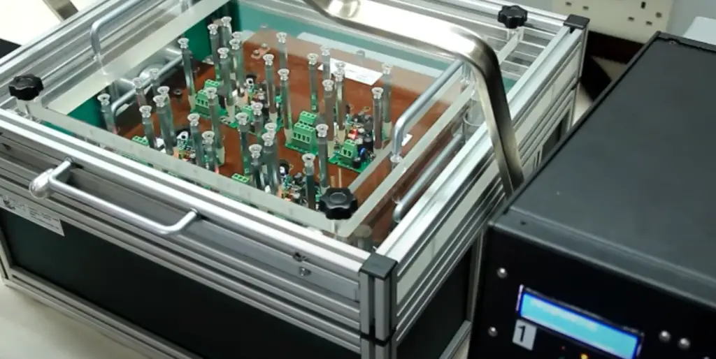
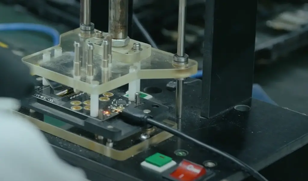
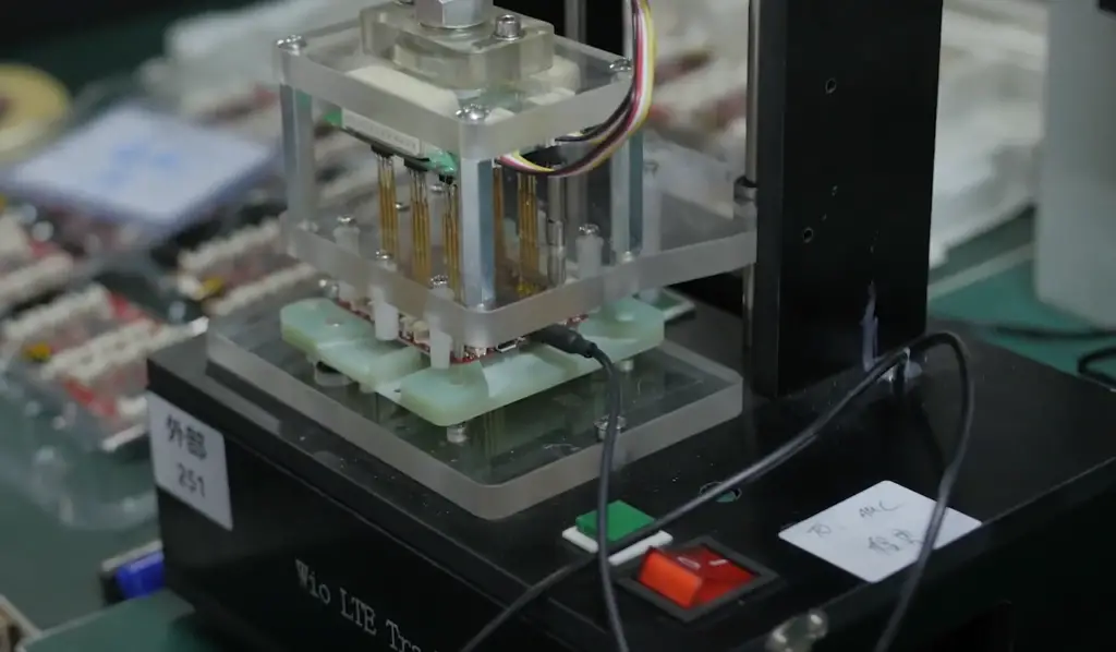
The most common model used for PCB testing is the “bed of nails” test fixture. This fixture consists of a grid of spring-loaded pins, which make contact with the test points on the PCB. The pins are arranged to match the pattern of the PCB, and the fixture is connected to a test system, which sends signals to the pins to test the components on the board.
11. What are the 3 functional tests?
3 functional tests are:
- Power-up test: This test checks if the device powers up and initializes correctly;
- Functional test: This test checks if the device performs its intended functions according to the specifications;
- Environmental test: This test checks if the device can operate under different environmental conditions such as temperature, humidity, and vibration [12];
12. What are the 4 levels of functional testing?
4 levels of functional testing are:
- Unit testing: This tests individual components or modules of the device;
- Integration testing: This tests how different components interact with each other;
- System testing: This tests the complete system to ensure that it meets the requirements and specifications;
- Acceptance testing: This tests the system with real-world data to ensure that it meets the user’s needs;
13. What is PCB assembly and testing?
PCB assembly and testing is the process of assembling and testing the electronic components on a printed circuit board. It involves mounting the components on the board, soldering them in place, and testing the functionality of the assembled board using various testing methods.
14. What are the 4 stages of PCB design flow?
4 stages of PCB design flow are:
- Schematic capture: This stage involves creating a schematic diagram that represents the components and their connections;
- Board layout: This stage involves placing the components on the board and routing the connections between them;
- Design rule checking: This stage involves verifying that the design meets the manufacturing rules and specifications;
- Gerber generation: This stage involves generating the Gerber files, which contain the information required for the manufacturing process, including the placement of components and the routing of connections on the PCB [13];
15. What are the two functions of PCB?
The two main functions of a PCB are to provide a platform for connecting electronic components and to provide a pathway for electrical signals to flow between those components. PCBs enable the efficient and reliable connection of components by using copper traces, vias, and pads to create electrical connections between components. They also help to reduce the size and complexity of electronic devices by allowing components to be densely packed on a single board.
16. How do you test a faulty PCB?
To test a faulty PCB, you can use various methods such as visual inspection, functional testing, and diagnostic testing:
- Visual inspection involves examining the board for any physical damage, such as cracks or broken components;
- Functional testing involves checking the components on the board to ensure that they are performing their intended functions;
- Diagnostic testing involves using specialized equipment, such as an oscilloscope or logic analyzer, to analyze the signals and communication between components on the board;
17. Where are the test points on a PCB?
Test points on a PCB are designated locations where a technician can connect test probes or other testing equipment to test or measure specific signals on the board. These points are typically designated with a circle or square pad on the board and are labeled with a reference designator, such as TP1, TP2, etc. Test points can be located anywhere on the board, but they are typically placed near critical components or signal paths for easy access during testing.
Useful Video: Functional Testing – PCB Assembly Testing Methods
References
- https://resources.altium.com/p/pcb-functional-testing-and-role-manufacturer-collaboration
- https://emsginc.com/resources/what-is-pcb-functional-testing/
- https://blog.matric.com/what-is-pcb-functional-testing
- https://www.nexlogic.com/pcb-testing/functional-testing/
- https://www.creativehitech.com/pcb-fabrication/pcb-functional-testing/
- https://www.7pcb.com/Functional-Testing
- https://madpcb.com/functional-testing/
- https://www.technotronix.us/pcb-functional-testing.html
- https://www.seeedstudio.com/blog/2021/06/18/pcba-functional-testing/
- https://www.rigiflex.com/pcb-functional-testing-services
- https://www.assemblymag.com/articles/83988-functional-testing-of-pcbs
- https://www.acceleratedassemblies.com/blog/role-of-functional-testing-in-pcb-assembly
- https://www.pcbway.com/pcb_prototype/PCB_Assembly_Functional_Testing.html