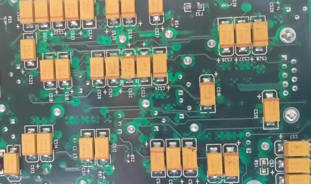
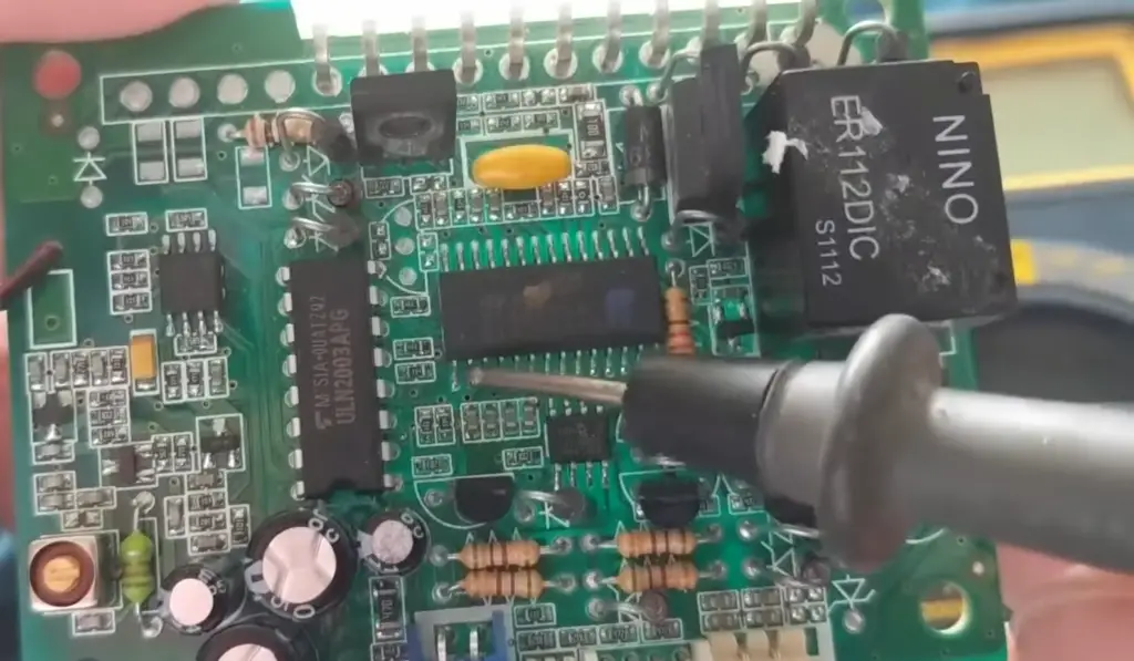
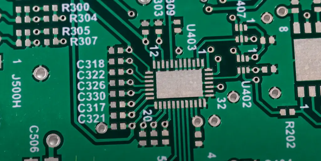
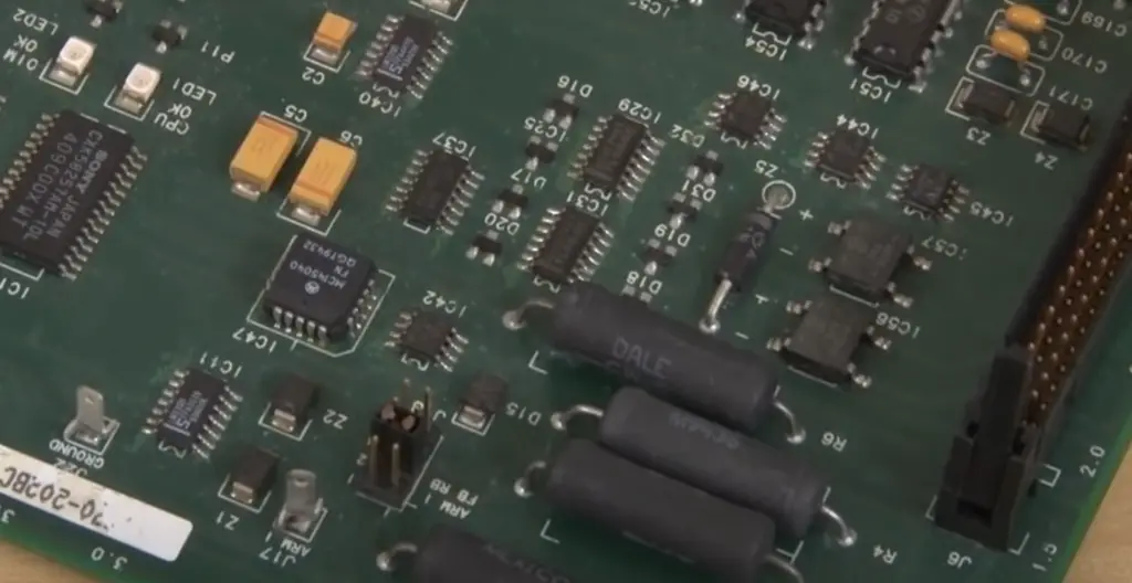
Printed Circuit Boards (PCBs) are the backbone of modern electronic devices, ranging from smartphones to aerospace systems. PCBs are composed of various components, such as resistors, capacitors, and integrated circuits, mounted on a substrate. The assembly and production of PCBs are critical processes that require careful attention to detail, as the failure of a single component can cause catastrophic consequences. Therefore, it is essential to ensure that PCBs are thoroughly tested before they are integrated into final products.
This article aims to provide an overview of the various PCB testing methods used in the industry. It will start by outlining the various stages of PCB testing, from design verification to functional testing. The article will then delve into the different testing techniques, such as visual inspection, automated optical inspection (AOI), X-ray inspection, and in-circuit testing (ICT). It will also discuss how each method works, its benefits, limitations, and typical applications [1].
Furthermore, the article will cover advanced PCB testing techniques, such as boundary scan testing, functional testing, and environmental testing. It will explain how these methods are used to evaluate a PCB’s functionality, reliability, and durability under various conditions. The article will also highlight the importance of testing PCBs to ensure product quality, reliability, and safety.
What Is PCB Testing and What Is Being Tested?
Printed Circuit Boards (PCBs) are an essential part of modern electronic devices. PCBs are made up of various components mounted on a substrate, and they allow for the efficient flow of electricity between different components. These components are connected through conductive pathways, commonly referred to as traces. The production and assembly of PCBs are crucial processes that must be done with great care and attention to detail. A single faulty component can cause severe consequences, ranging from device malfunction to safety hazards. [2]
PCB testing is the process of verifying that a PCB meets its design specifications and functions correctly. The primary objective of PCB testing is to identify any manufacturing defects or design flaws that may affect the PCB’s functionality. PCB testing is a complex process that involves several stages, ranging from design verification to functional testing. Various testing techniques are employed to detect and isolate faults in a PCB, including visual inspection, automated optical inspection (AOI), X-ray inspection, and in-circuit testing (ICT).
Each method has its benefits and limitations, and the appropriate technique is chosen based on the specific requirements of the application.
Why PCB Testing Is Necessary?
PCB testing is necessary for several reasons:
- First and foremost, PCB testing ensures the reliability and safety of electronic products. A single faulty component can cause a device to malfunction, leading to safety hazards, loss of revenue, and damage to the brand’s reputation. PCB testing helps to identify and isolate these faults before the product reaches the market, ensuring that the final product is safe and reliable;
- Secondly, PCB testing helps to reduce production costs by minimizing the number of faulty PCBs produced. Faulty PCBs not only lead to product recalls and lost revenue but also increase the production cost per unit. By identifying faults early in the production process, manufacturers can reduce the number of faulty PCBs produced, leading to significant cost savings;
- Lastly, PCB testing helps to ensure that the final product meets regulatory requirements. Regulatory bodies such as the International Electrotechnical Commission (IEC) and the International Organization for Standardization (ISO) have specific requirements that electronic products must meet. PCB testing ensures that the final product meets these requirements, allowing the product to be sold in various regions globally [3];
Benefits of PCB Testing
Ensuring Product Reliability and Safety
The primary benefit of PCB testing is that it ensures the reliability and safety of electronic products. Faulty PCBs can cause a device to malfunction, leading to safety hazards, loss of revenue, and damage to the brand’s reputation. PCB testing helps to identify and isolate these faults before the product reaches the market, ensuring that the final product is safe and reliable.
Reducing Production Costs
PCB testing helps to reduce production costs by minimizing the number of faulty PCBs produced. Faulty PCBs not only lead to product recalls and lost revenue but also increase the production cost per unit. By identifying faults early in the production process, manufacturers can reduce the number of faulty PCBs produced, leading to significant cost savings.
Improving Product Quality
PCB testing helps to improve product quality by identifying faults early in the production process. By detecting and isolating faults early, manufacturers can improve the production process, leading to higher-quality products.
Meeting Regulatory Requirements
Regulatory bodies such as the International Electrotechnical Commission (IEC) and the International Organization for Standardization (ISO) have specific requirements that electronic products must meet. PCB testing ensures that the final product meets these requirements, allowing the product to be sold in various regions globally.
Identifying Design Flaws
PCB testing helps to identify design flaws early in the development process. By identifying design flaws early, manufacturers can make necessary changes to improve the overall design and functionality of the product. This leads to the production of more efficient and reliable electronic products.
Ensuring Consistency in Production
PCB testing helps to ensure consistency in the production process. By testing each PCB, manufacturers can ensure that each unit produced meets the same specifications and requirements. This leads to greater consistency in the production process and a higher-quality final product.
Enhancing Customer Satisfaction
PCB testing helps to enhance customer satisfaction by ensuring that electronic products are safe, reliable, and of high quality. By identifying and isolating faults before the product reaches the market, manufacturers can prevent product recalls and improve the overall customer experience [4].
Major Types of PCB Testing Methods
1) In-Circuit Testing (ICT)
This method is conducted when the PCB is still in its assembly phase, and it is used to check for any faults in the circuitry of the PCB. The testing equipment used in this method is designed to make contact with specific points on the PCB and measure the electrical performance of the board.
ICT is a quick and efficient method of testing PCBs, and it is often used in high-volume manufacturing. The downside of this method is that it can only detect faults that affect the electrical performance of the PCB and not physical defects.
2) Flying Probe Testing
Flying Probe Testing is a type of PCB testing that uses a specialized piece of equipment to make contact with specific points on the PCB and measure its electrical performance. The equipment used in this method does not require any physical contact with the PCB, hence the name “flying probe”. This makes it an ideal method for testing PCBs that have complex and delicate components.
The downside of this method is that it is slower than In-Circuit Testing, and it cannot detect certain types of faults, such as those caused by a missing component or a wrong polarity.
3) Automated Optical Inspection (AOI)
Automated Optical Inspection (AOI) is a type of PCB testing that uses cameras to inspect the PCB for defects. The cameras capture images of the PCB, and specialized software is used to analyze the images and detect any defects. This method is used to check for missing or incorrect components, solder defects, and other physical defects on the PCB.
AOI is a fast and accurate method of testing PCBs, and it is often used in high-volume manufacturing. The downside of this method is that it cannot detect faults that affect the electrical performance of the PCB.
4) Burn-In Testing
Burn-In Testing is a type of PCB testing that involves subjecting the PCB to high temperatures and electrical stresses to simulate the conditions it will experience during its lifetime. This method is used to detect any faults that may occur over time due to temperature changes, electrical stress, or other environmental factors.
Burn-In Testing is a time-consuming method, and it is often used for high-reliability applications, such as aerospace and medical equipment. The downside of this method is that it cannot detect certain types of faults, such as those caused by a missing component or a wrong polarity [5].
5) X-Ray Inspection
X-Ray Inspection is a type of PCB testing that uses X-rays to inspect the PCB for defects. The X-rays are passed through the PCB, and specialized software is used to analyze the images and detect any defects. This method is used to check for missing or incorrect components, solder defects, and other physical defects on the PCB.
X-Ray Inspection is a non-destructive method of testing PCBs, and it can detect faults that cannot be detected by other methods. The downside of this method is that it is expensive and time-consuming.
6) Functional Testing
Functional Testing is a type of PCB testing that involves testing the PCB under actual operating conditions. This method is used to check the performance of the PCB under real-world conditions and to detect any faults that may not be detected by other methods.
Functional Testing is a comprehensive method of testing PCBs, and it can detect faults that cannot be detected by other methods. The downside of this method is that it is time-consuming and requires specialized equipment.
7) Boundary Scan Testing
Boundary Scan Testing is a type of PCB testing that involves the use of a specialized chip called a boundary scan cell. The boundary scan cell is integrated into the PCB and can be used to test the connectivity and functionality of the PCB. This method is often used in complex PCBs with high pin counts.
Boundary Scan Testing is a fast and efficient method of testing PCBs, and it can detect faults that cannot be detected by other methods. The downside of this method is that it requires specialized equipment and can be challenging to set up.
8) Inspection by Humans
Inspection by Humans is a type of PCB testing that involves visually inspecting the PCB for defects. This method is often used in low-volume manufacturing or for prototypes. It is a time-consuming method, but it can detect physical defects that cannot be detected by other methods.
9) GM/LTS
GM/LTS (Gate Matrix/Low-Temperature Storage) is a type of PCB testing that involves the use of specialized equipment to measure the electrical performance of the PCB at different temperatures. This method is used to check for any changes in the electrical performance of the PCB due to temperature changes.
GM/LTS is a comprehensive method of testing PCBs, and it can detect faults that cannot be detected by other methods. The downside of this method is that it requires specialized equipment and can be time-consuming [6].
10) Time Domain Reflectometry Test (TDR)
Time Domain Reflectometry Test (TDR) is a type of PCB testing that involves the use of specialized equipment to measure the electrical performance of the PCB. This method is used to check for any faults in the signal transmission lines of the PCB.
TDR is a fast and efficient method of testing PCBs, and it can detect faults that cannot be detected by other methods. The downside of this method is that it requires specialized equipment and can be challenging to set up.
11) Resistivity of the Solvent Extract Test (ROSE)
The resistivity of the Solvent Extract Test (ROSE) is a type of PCB testing that involves the use of specialized equipment to measure the electrical resistance of the PCB. This method is used to check for any contamination on the PCB that may affect its electrical performance.
ROSE is a comprehensive method of testing PCBs, and it can detect faults that cannot be detected by other methods. The downside of this method is that it requires specialized equipment and can be time-consuming.
12) Aging Test
Aging Test is a type of PCB testing that involves subjecting the PCB to stress over an extended period to simulate the conditions it will experience during its lifetime. This method is used to check for any faults that may occur due to aging, such as changes in the electrical performance of the PCB or physical defects.
Aging Test is a time-consuming method, and it is often used for high-reliability applications, such as aerospace and medical equipment. The downside of this method is that it cannot detect certain types of faults, such as those caused by a missing component or a wrong polarity.
13) Laser Detection
Laser Detection is a type of PCB testing that involves the use of a laser to detect faults in the PCB. This method is used to check for any physical defects in the PCB, such as cracks or breaks in the circuitry.
Laser Detection is a quick and efficient method of testing PCBs, and it can detect faults that cannot be detected by other methods. The downside of this method is that it requires specialized equipment and can be challenging to set up.
Common Defects in Circuit Board Testing
Opens and Shorts
An open circuit occurs when a break occurs in the conductive path of the PCB. It results in a loss of connectivity between two points. A short circuit occurs when two conductive paths are accidentally connected, resulting in a current flowing between them. These defects can occur due to poor design or manufacturing practices.
Soldering Defects
Soldering is a critical process in PCB assembly. Soldering defects occur when the solder does not form a good connection between the component and the PCB. These defects can lead to intermittent connectivity or a complete loss of connectivity between components.
Component Defects
Component defects can occur due to poor handling practices, such as electrostatic discharge or incorrect storage conditions. These defects can result in components not functioning correctly, leading to device failure.
Incorrect Component Placement
Incorrect component placement can result in circuit board failure. It can cause a short circuit or a break in the conductive path [7].
Inspection Methods
Various inspection methods are used to detect defects in circuit boards. These methods include:
- Visual Inspection. Visual inspection involves manually checking the circuit board for any defects. This method is quick and easy, but it is not as effective as other methods;
- Automated Optical Inspection (AOI). AOI is a non-contact, high-speed inspection method used to detect defects in circuit boards. It uses cameras to inspect the board and detect defects such as opens, shorts, and incorrect component placement;
- X-ray Inspection. X-ray inspection is used to detect internal defects in the circuit board, such as solder joint quality and component placement. It is a non-destructive testing method and can be used to inspect multilayer PCBs;
Detection of Defects
The detection of defects can be challenging, and it often requires a combination of inspection methods. In-circuit testing and functional testing are two methods used to detect defects in circuit boards.
In-circuit testing involves checking the circuit board while it is still in the device. It checks the functionality of the device and detects any open or short circuits. This method is used for high-volume production, and it is an effective way to detect defects in the early stages of production.
Functional testing involves checking the functionality of the device under different conditions. It tests the device under various environmental conditions, such as temperature and humidity. This method is time-consuming and expensive, but it is an effective way to detect defects that may not be detected by other methods [8].
Cost of Repairs
The cost of repairing a faulty circuit board depends on the type and severity of the defect. Minor defects such as opens and shorts can be repaired easily and at a low cost. Soldering defects and incorrect component placement can also be repaired, but it may require more time and effort. Component defects and internal defects can be challenging and expensive to repair. In some cases, it may be more cost-effective to replace the entire circuit board rather than repair it.
FAQ
1. What are the 3 types of PCB?
There are 3 types of PCB: Single-sided PCB, Double-sided PCB, and Multi-layer PCB. Single-sided PCBs have copper conductive material on one side of the board, while double-sided PCBs have copper conductive material on both sides of the board. Multi-layer PCBs are composed of several layers of conductive material, typically between 4-10 layers. [9]
2. What are the 3 methods of PCB designing?
The three methods of PCB designing are:
- Manual designing: involves drawing the circuit diagram on paper and then transferring it onto the PCB board;
- Computer-Aided Design (CAD): involves using specialized software to design the PCB and its components;
- Auto-routing: involves automated routing of connections between components using software;
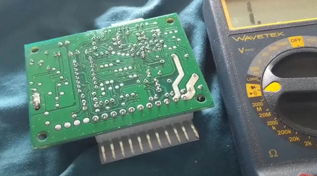
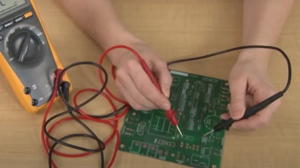
3. How do you test a PCB with a multimeter?
To test a PCB with a multimeter, set the multimeter to continuity mode and touch the probes to the corresponding points on the PCB to check for continuity.
4. How do you test a faulty PCB?
A faulty PCB can be tested by checking for continuity, resistance, and voltage using a multimeter. Other tests can include visual inspections for damage, thermal imaging, and functional testing with specialized equipment.
5. What are the 4 layers of PCB?
Four layers of PCB are:
- Top layer: this is the layer where the components are mounted and connected to the PCB;
- Bottom layer: this layer contains the copper traces that connect the components;
- Power plane layer: this layer provides a stable voltage source to the components on the PCB;
- Ground plane layer: this layer provides a stable ground reference for the components on the PCB [10];
6. Is PCB mechanical or electrical?
PCBs are primarily electrical, as they are designed to provide a means of electrical connection between components. However, mechanical considerations such as board thickness, mounting holes, and component placement are also important aspects of PCB design.
7. What is standard PCB thickness?
The standard thickness of a PCB is typically between 0.6mm to 1.67 mm (0.062 inches). However, thicker PCBs may be required for specialized applications that require greater durability or heat dissipation.
8. What are the 5 types of functional testing?
5 types of functional testing for PCBs are:
- Continuity testing: checking for continuity between points on the PCB to ensure proper electrical connections;
- Resistance testing: measuring the resistance between points on the PCB to ensure proper circuit function;
- Voltage testing: measuring the voltage between points on the PCB to ensure proper power supply to components;
- Signal integrity testing: testing the quality and integrity of signals transmitted across the PCB;
- Environmental testing: testing the PCB under various environmental conditions to ensure proper function under different operating conditions [11];
9. What is PCB assembly and testing?
PCB assembly involves the process of mounting and soldering components onto the PCB board. PCB testing involves testing the assembled board for proper function and electrical connections.
10. What is QA functional testing?
This can involve a range of tests, including functional testing, environmental testing, and electrical testing [12].
11. What is PCB test equipment?
PCB test equipment refers to specialized equipment used for testing PCBs, including multimeters, oscilloscopes, function generators, and specialized test fixtures.
12. What is the importance of PCB testing?
PCB testing is important to ensure that electronic products are safe, reliable, and of high quality. Faulty PCBs can lead to product failure, electrical fires, and even injury or death in some cases. PCB testing helps to identify any issues or faults in the board before it is used in a product, ensuring that it is safe and reliable for use [13].
13. Can PCB be any size?
PCBs can be manufactured in various sizes, depending on the requirements of the application. However, there may be limitations to the size of the PCB based on the manufacturing process and equipment used [14].
14. What are PCB standards?
PCB standards are a set of guidelines and requirements that specify the design, manufacturing, and testing of PCBs. These standards help to ensure that PCBs are safe, reliable, and of high quality, and may be set by industry associations or regulatory bodies. Some common PCB standards include IPC-A-600 for visual inspection, IPC-6012 for fabrication, and IPC-610 for assembly. [15]
Useful Video: HOW TO UNDERSTAND A PRINTED CIRCUIT BOARD AND IT’S CONNECTIONS
References
- https://blog.matric.com/pcb-testing-methods
- https://www.seeedstudio.com/blog/2021/06/18/7-most-popular-pcb-testing-methods-during-manufacturing-and-assembly/
- https://www.mclpcb.com/blog/pcb-testing-methods-guide/
- https://www.proto-electronics.com/blog/an-overview-of-pcb-testing-and-inspection-methods
- https://www.raypcb.com/circuit-card-assembly-testing/
- https://resources.altium.com/ru/p/pcb-testing-101-important-methods-and-metrics
- https://jhdpcb.com/pcb-testing/
- https://tempoautomation.com/blog/circuit-board-testing-methods-for-pcb-manufacturing/
- https://aapcb.com/blog/seven-types-of-pcb-testing-methods-what-you-need-to-know/
- https://www.pcbnet.com/blog/a-guide-to-pcb-testing-methods/
- https://www.twistedtraces.com/blog/know-the-types-of-pcb-testing-methods
- http://www.cubixcontrolsystems.com/7_PCB_testing_methods_you_need_to_know.html
- https://www.linkedin.com/pulse/pcb-testing-methods-validate-manufacturing-jeff-trambley
- https://www.nextpcb.com/blog/13-popular-pcb-test-methods
- https://www.gadgetronicx.com/pcb-testing-methods/