
Printed Circuit Board (PCB) manufacturing is a crucial process in the production of electronic devices, ranging from small consumer electronics to complex aerospace systems. PCBs are the backbone of modern electronics, allowing for efficient and reliable connections between electronic components.
The PCB manufacturing process involves a series of complex steps, including designing the PCB layout, etching the copper-clad laminate, drilling holes for components, applying solder mask and silk screen, and quality testing the final product. Each step is critical to ensure that the PCB meets the required specifications, performs reliably, and is cost-effective.
In recent years, there has been an increased demand for smaller and more complex electronic devices, which has led to the need for more advanced PCB manufacturing processes. The use of new technologies, such as laser drilling and 3D printing, has enabled manufacturers to produce smaller, more intricate PCBs, while also reducing production costs.
Furthermore, the adoption of Industry 4.0 principles, including automation and machine learning, has streamlined the PCB manufacturing process, resulting in increased efficiency and productivity.
What is the PCB Manufacturing Process?
The Printed Circuit Board (PCB) manufacturing process is a complex one that involves several steps and stages. It starts with the fabrication of the PCB, which is created by a combination of image transfer, etching, plating, drilling, and other processes to create the desired circuit pattern on the board [1].
Once this is complete, components are mounted onto the board using solder paste and reflow soldering techniques. This mounting step is followed by electrical testing to ensure that all connections work correctly.
Finally, additional layers of insulation material may be added if needed before the PCBs go through final inspection prior to shipment.
The PCB manufacturing process includes several important steps in order to ensure quality control throughout each stage of production:
- First off, the PCBs need to be designed accurately and thoroughly. This requires that a CAD program is used in order to ensure that all dimensions and components are accounted for;
- Once the design has been completed and approved, the materials required for fabrication can be sourced. These include copper-clad boards, etchants, soldering materials, and other components as needed;
- Next, comes the fabrication process itself. The PCB is first exposed to an image transfer process that uses light-sensitive chemicals in order to create a precise circuit pattern on the board. Next, an etching process is used to remove excess copper from the board before plating is applied for electrical conduction purposes. Drilling follows this step in order to cut holes into the board where components will be mounted. After these steps are complete, the board is ready for component mounting and testing;
What Are The Parts of a PCB?
A typical PCB consists of several parts, each serving a specific purpose in the circuit design [2].
The parts of a PCB include:
- Substrate: The substrate is the base material on which the PCB is built. It can be made of various materials, including fiberglass, ceramic, or even plastic. The substrate provides support for the copper layers, components, and connections;
- Copper Layers: Copper layers are thin sheets of copper that are laminated to the substrate. These copper layers serve as the conductive pathways for the circuit. The copper layers are etched to create the desired circuit pattern;
- Solder Mask: A solder mask is a thin layer of polymer material that is applied to the surface of the PCB to protect the copper traces from damage and prevent solder bridges between adjacent connections during the assembly process;
- Silk Screen: The silk screen layer is used to print the component names, values, and reference designators on the PCB. This layer is typically applied using a white ink that contrasts well with the green solder mask;
- Components: Components are the individual electronic devices that are mounted on the PCB. These components can include resistors, capacitors, diodes, transistors, and integrated circuits;
- Through Holes: Through holes are drilled holes that extend through the substrate and copper layers of the PCB. These holes allow for the insertion of components and the creation of connections between the layers;
- Via Holes: Via holes are similar to through holes but are used to connect the copper layers within the PCB, rather than extending through the entire board;
- Pads: Pads are the copper areas on the PCB that are used to create connections between the components and the copper layers;
How to Implement an Effective PCB Manufacturing Process:
Gather Components
The first step in any PCB manufacturing process is to gather the components that will be used to build the board. These components can include resistors, capacitors, transistors, and integrated circuits. It is important to ensure that all components are of the correct type and value, as well as being compatible with each other and the board design.
One key consideration when gathering components is lead time. Many components have long lead times, which can delay the manufacturing process. It is important to plan ahead and order components as early as possible to avoid delays.
Another important consideration is the quality of the components. Low-quality components can lead to reliability issues and may cause the board to fail prematurely. It is important to source components from reputable suppliers and to perform quality checks before using them in the manufacturing process.
Design for Manufacturing (DFM) Considerations
This includes considerations such as component placement, trace routing, and board size. By designing for manufacturing, it is possible to reduce the cost and complexity of the manufacturing process, as well as improve the reliability and performance of the final product.
One key consideration when designing for manufacturing is component placement. Components should be placed in a logical and efficient manner to minimize the length of traces and reduce the complexity of the routing process. This can help to reduce the overall size of the board, as well as minimize the number of layers required [3].
Another important consideration is trace routing. Traces should be routed in a way that minimizes crosstalk, signal degradation, and electromagnetic interference (EMI). This can be achieved by using ground planes, signal isolation, and careful placement of components.

Board Materials
The choice of board materials can have a significant impact on the performance and reliability of a PCB. There are a wide variety of materials available, each with its own advantages and disadvantages.
Common board materials include FR4, Rogers, and ceramic:
- FR4 is the most commonly used board material and is suitable for most applications. It is a fiberglass-reinforced epoxy laminate that is easy to work with and relatively inexpensive. FR4 is also highly resistant to heat, making it ideal for use in high-temperature applications;
- Rogers is a high-performance board material that is used in applications where reliability and performance are critical. It is more expensive than FR4 but offers superior electrical performance, including low dielectric loss and high thermal conductivity. Rogers is also highly resistant to temperature and moisture, making it ideal for use in harsh environments;
- Ceramics is another high-performance board material that is used in applications where extreme reliability and performance are required. It is more expensive than FR4 and Rogers but offers superior electrical performance, including high dielectric strength and low dielectric loss. Ceramic is also highly resistant to heat, making it ideal for use in high-temperature applications [4];
File Formats
The final key consideration in implementing an effective PCB manufacturing process is file formats. PCB designs are typically created using specialized software such as Altium Designer or Eagle. These software packages generate files in a variety of formats, including Gerber, Excellon, and ODB++.
Excellon is a file format that contains the information required to create the drill files for the PCB. This includes the position, size, and shape of each hole on the board. Excellon files can be generated by most PCB design software and are compatible with most PCB manufacturing processes.
ODB++ is a newer file format that is gaining popularity in the PCB manufacturing industry. It is a comprehensive file format that contains all of the information required to create the board, including the copper layers, drill files, silk screen, and bill of materials. ODB++ files can be generated by most PCB design software but may require additional software to be used by PCB manufacturers.
In addition to these file formats, it is also important to consider the version control and revision management of the PCB design files. It is important to keep track of changes made to the design files and to ensure that the latest version is always used in the manufacturing process [5].
What is the Difference Between PCB Fabrication and PCB Assembly Process?
The PCB fabrication process is the process of creating printed circuit boards. This involves applying conductive layers of metal (usually copper) onto an insulated board and etching away unwanted metal to create electrical pathways between components. The main goal of the fabrication process is to ensure that all electrical connections are properly made and that the end product meets the design specifications.
PCB assembly, on the other hand, is a completely different step in manufacturing printed circuit boards. It involves taking individual electronic components and soldering them onto a completed PCB. This helps to create a functional printed circuit board with all its desired functionality. Unlike fabrication, it does not involve any intricate metal etching or coppering but rather focuses on assembling the various parts together in the correct order.
The difference between these two processes is mainly in the way they have carried out and the goals that each process is meant to achieve. PCB fabrication is a more involved process and usually takes more time and resources compared to assembly, while assembly focuses on taking pre-fabricated components and putting them together quickly and efficiently.
Steps Before Starting the PCB Fabrication Process:
1) Design Review
The first step before starting the PCB fabrication process is to review the design of the PCB. This involves checking the design for any errors or issues that could impact the functionality of the final product. This can be done using software tools that can identify any design rule violations, errors, or inconsistencies.
2) File Preparation
The next step is to prepare the files that will be used in the fabrication process. This includes converting the design files into the appropriate formats that can be used by the manufacturer. It is important to ensure that the files are complete and accurate and that all necessary information is included.
3) Material Selection
The next step is to select the materials that will be used in the fabrication process. This includes selecting the type of PCB substrate, the type of copper foil, and any other materials that will be used in the fabrication process. The materials selected should meet the desired specifications and requirements for the final product.
4) Panelization
Panelization is the process of arranging multiple PCBs on a single panel for fabrication. This can help reduce costs and improve efficiency in the fabrication process. The panelization process involves designing the layout of the PCBs on the panel and generating the necessary files for fabrication.
5) Manufacturer Selection
The final step before starting the PCB fabrication process is to select the manufacturer that will be used to produce the PCBs. This involves evaluating different manufacturers based on their experience, capabilities, quality control processes, customer service, and pricing. It is important to select a manufacturer that can meet the desired specifications and requirements for the final product, while also providing a high level of quality and service [6].
PCB Design Process
Schematic Design
The schematic design is the first stage of the PCB design process. In this stage, the circuit’s functional diagram is created using a schematic capture tool, such as Altium Designer or Eagle. The schematic design helps engineers visualize the connections between components, analyze the circuit’s behavior, and detect potential errors before proceeding to the PCB layout.
At this stage, the engineer must consider the circuit’s intended function, the components needed to achieve that function, and the physical constraints of the PCB. The schematic should also adhere to industry standards and design rules, such as trace widths, clearances, and signal integrity requirements.
PCB Layout Planning
Once the schematic design is completed, the next stage is to plan the PCB layout.
During the PCB layout planning stage, the engineer must consider the board’s size, shape, and number of layers. They must also decide on the placement of components and the routing of the traces. The layout planning should also adhere to design rules, such as minimum clearances, signal integrity constraints, and power distribution considerations.
Component Placement Planning
The component placement planning stage is where the engineer decides on the exact position of each component on the PCB. The placement affects the circuit’s performance, reliability, and ease of manufacturing.
The engineer must consider factors such as signal integrity, thermal management, and mechanical stability when placing components. They must also ensure that there is enough space between components for routing and assembly. It is also important to group similar components together to minimize noise and interference.
Connection Routing
After the component placement planning is complete, the next stage is to route the connections between the components. The routing stage involves creating the physical copper traces that connect the components on the PCB.
The engineer must consider several factors when routings, such as signal integrity, power distribution, and thermal management. They must also ensure that the routing adheres to the design rules, such as minimum trace widths, clearances, and impedance control.
Designing the Circuit Board
The PCB design process’s most critical stage is designing the circuit board. In this stage, the engineer must ensure that the PCB design meets the functional and performance requirements and adheres to the industry standards and design rules.
The engineer must review the PCB design thoroughly, looking for potential errors or design rule violations. They must also perform a Design for Manufacturability (DFM) analysis to ensure that the PCB can be manufactured efficiently and without errors.
Final Manufacturing Files
The final stage of the PCB design process is preparing the manufacturing files. These files contain all the information necessary for the PCB manufacturer to produce the PCB, such as the Gerber files, drill files, and assembly instructions.
The engineer must ensure that the manufacturing files are accurate, complete, and adhere to the industry standards and design rules. They must also provide clear instructions to the manufacturer on how to assemble and test the PCB.
PCB Manufacturing Process:
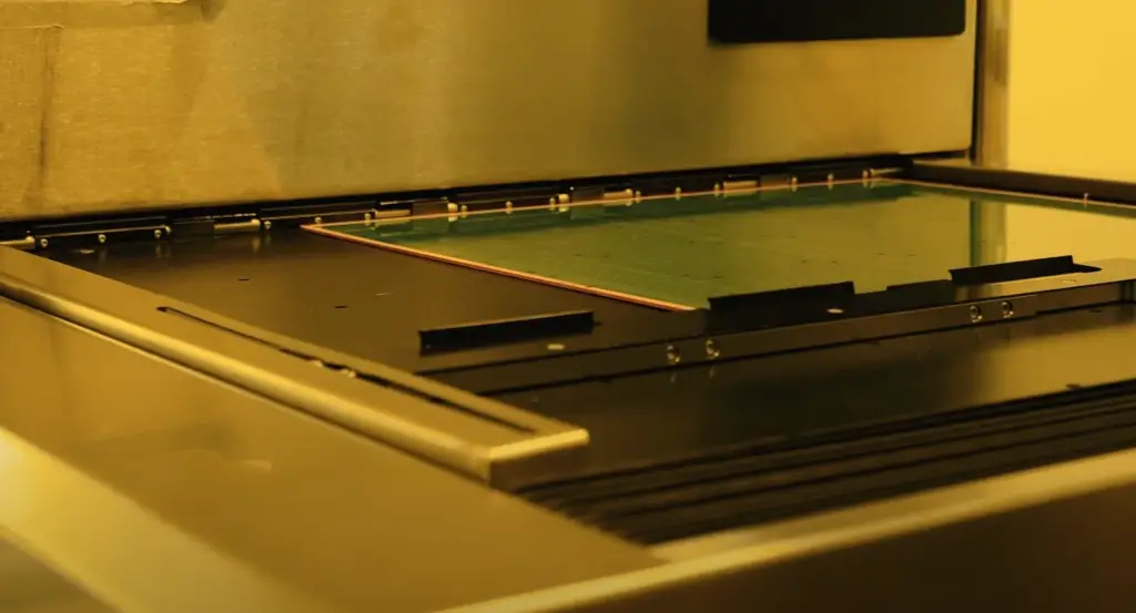
1. Imaging the Design
The PCB manufacturing process begins with imaging the design onto a glass plate using a photolithography process. The glass plate is coated with a photoresist material, and the PCB design is printed onto the photoresist using a high-resolution printer.
2. Printing Inner Layers on Copper
In the next stage, the design is printed onto a copper-clad board using a printer. The printer uses a special ink that is resistant to the etching process, creating a protective layer on the copper.
3. UV Light Blasting
Once the design is printed onto the copper, the board is exposed to UV light. The UV light hardens the protective ink, making it resistant to the etching process.
4. Etching the Inner Layer
The next stage is to etch the inner layer. The board is soaked in an etching solution that removes the unprotected copper, leaving behind the circuit pattern.
5. Layer Alignment
In the layer alignment stage, the inner layers are aligned and laminated together using heat and pressure.
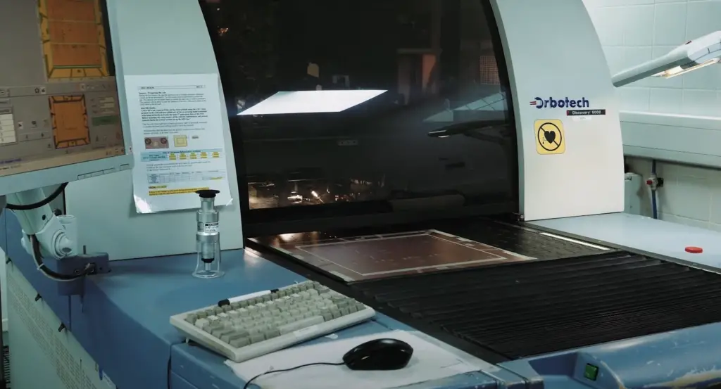
6. Optical Inspection
The laminated layers are then inspected optically for any defects or alignment issues.
7. Laminating & Pressing the Layers
The layers are then laminated and pressed together using heat and pressure to create a single board.
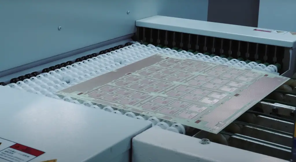
8. Drilling
In the drilling stage, the holes are drilled into the board to create the vias and through holes for component leads.
9. PCB Plating
After drilling, the PCB is plated with a thin layer of copper to provide better electrical conductivity and prevent corrosion [7].
10. Outer Layer Imaging
In the outer layer imaging stage, the PCB design is imaged onto the copper layer of the outer layer using a photolithography process.
11. Outer Layer Etching
The outer layer is then etched to remove the unprotected copper, leaving behind the circuit pattern.
12. Solder Mask Application
The solder mask is applied to the PCB to protect the copper traces and vias from oxidation and contamination during soldering.
13. Silk Screening
The PCB is then silk-screened with component designators, logos, and other markings.
14. Surface Finishing
In the surface finishing stage, the PCB is coated with a layer of metal, such as gold or silver, to improve its electrical properties and protect it from corrosion.
15. Testing
The PCB is then tested for electrical continuity and functionality. Testing involves checking each component for correct operation and verifying the correct connections between components.
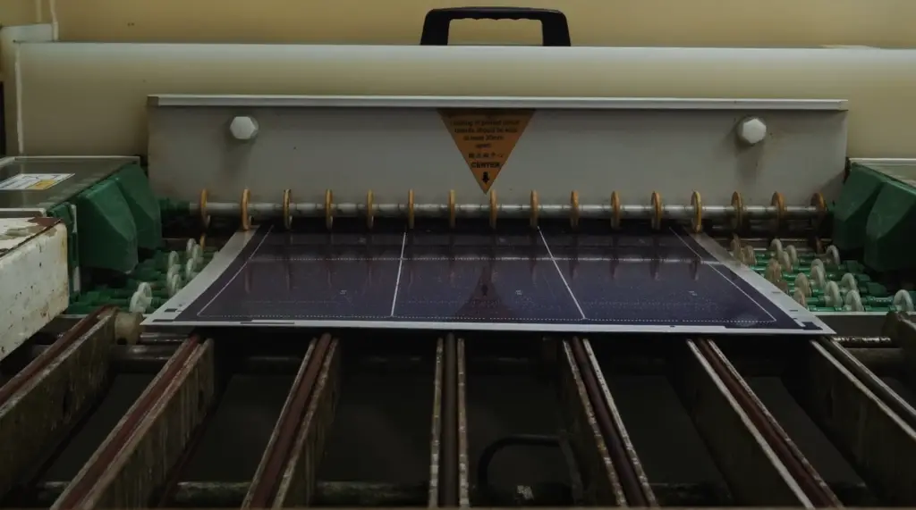
16. Profiling
In the profiling stage, the PCB is cut to its final dimensions using a machine that follows the PCB’s contours.
17. Final Quality Check
The final quality check involves inspecting the PCB for any defects or issues that may have arisen during the manufacturing process.
PCB Assembly Process:
Solder Paste Application
The first stage of the PCB assembly process is the application of solder paste onto the surface-mount components. Solder paste is a mixture of small solder balls and flux that is applied to the pads of the PCB where the components will be placed.
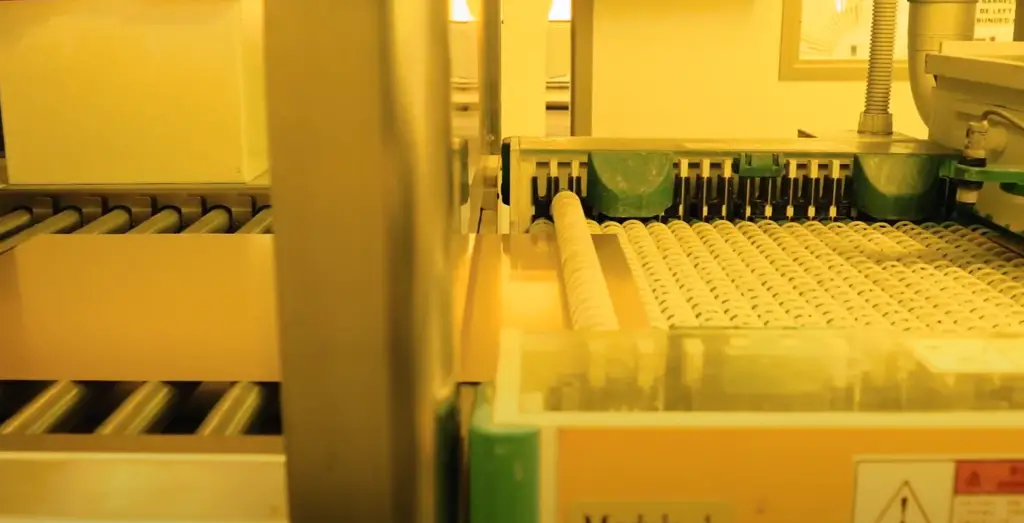
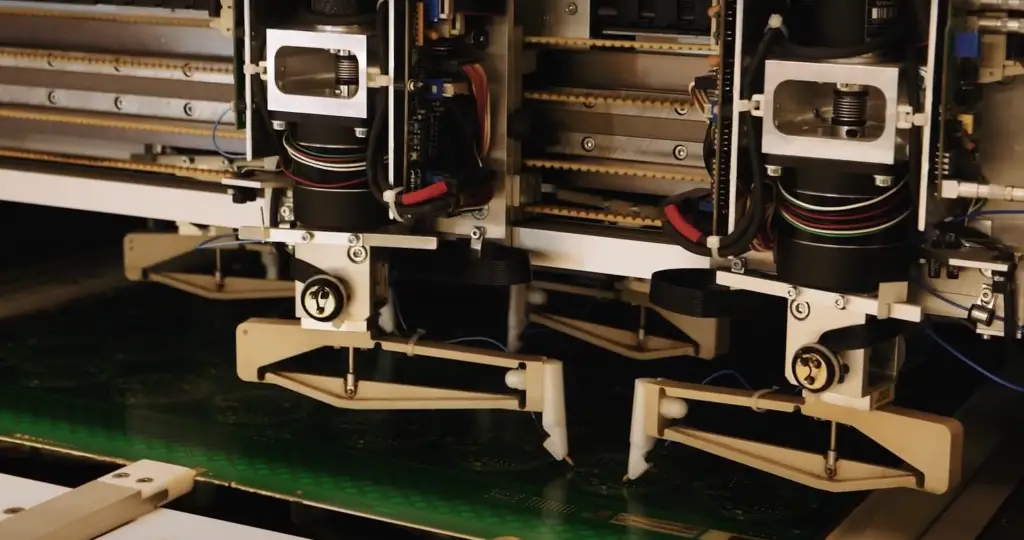
Pick and Place
The second stage of the PCB assembly process is the pick and place process. In this stage, the surface-mount components are placed onto the PCB using a pick-and-place machine. The machine uses a vacuum to pick up each component and place it onto the appropriate pad.
Reflow Soldering Process
The third stage of the PCB assembly process is the reflow soldering process. In this stage, the PCB is passed through a reflow oven where the solder paste is heated to melt and fuse the components onto the PCB. The oven uses a controlled temperature profile to prevent damage to the components.
Inspection
The fourth stage of the PCB assembly process is the inspection stage. In this stage, the PCB is inspected for any defects, such as misaligned components or soldering defects. Automated optical inspection (AOI) machines are used to check for defects in real time, ensuring high-quality assembly.
Plated Through Hole Component Insertion
The fifth stage of the PCB assembly process is the insertion of plated through-hole (PTH) components. PTH components are inserted into the holes drilled through the PCB, and their leads are soldered onto the opposite side of the PCB using a wave soldering machine.
Final Test and Inspection
The sixth stage of the PCB assembly process is the final test and inspection stage. In this stage, the completed PCB is tested for functionality and quality. The circuit is powered on, and the performance of each component is checked. The PCB is also visually inspected for any defects or issues.
Packaging and Shipping
The final stage of the PCB assembly process is the packaging and shipping stage. The PCB is carefully packaged to protect it from damage during transportation and storage. The packaging must be designed to meet industry standards and customer requirements.
Considerations for the PCB Fabrication Process
During the PCB assembly process, several factors must be considered to ensure a high-quality product. These factors include the design of the PCB, the selection of components, the selection of the assembly process, and the testing process. Other factors that affect the assembly process include the environment, such as temperature and humidity, and the quality of the equipment used.
How to Choose the Right PCB Manufacturer?
Choosing the right PCB manufacturer is an important decision that can have a significant impact on the quality and reliability of your product. With so many manufacturers to choose from, it can be difficult to know which one to select. In this article, we will discuss some key factors to consider when choosing a PCB manufacturer.
Experience and Expertise
One of the most important factors to consider when choosing a PCB manufacturer is their experience and expertise. Look for a manufacturer that has been in business for a number of years and has a proven track record of producing high-quality products. Check to see if the manufacturer has experience working with products similar to yours, and if they have any relevant certifications or industry affiliations.
Capabilities
Another important factor to consider is the manufacturer’s capabilities. Look for a manufacturer that has the equipment and expertise to produce the type of PCB that you need. Consider the manufacturer’s ability to handle large or small production runs, their turnaround times, and their ability to handle complex designs or specific requirements [8].
Quality Control
Ask about their testing procedures, inspection processes, and any certifications or quality control standards that they follow.
Customer Service
Customer service is another important factor to consider when choosing a PCB manufacturer. Look for a manufacturer that is responsive, communicative, and easy to work with. Consider their ability to answer questions, provide updates, and resolve any issues that may arise.
Pricing
Pricing is, of course, an important consideration when choosing a PCB manufacturer. Look for a manufacturer that offers competitive pricing while still maintaining high-quality standards. Consider any additional costs, such as shipping or setup fees, when comparing pricing.
Location
Finally, consider the location of the PCB manufacturer. Look for a manufacturer that is conveniently located for your business, as this can help reduce shipping costs and turnaround times. However, it is also important to consider the quality of the manufacturer’s products and services, so don’t choose a manufacturer based solely on location.
FAQ
1. What are the main components of a PCB?
The main components of a PCB (Printed Circuit Board) include a substrate, copper layers, solder mask, silk screen, components, through holes, via holes, and pads.
The substrate serves as the base material on which the PCB is built, while copper layers provide the conductive pathways for the circuit. The solder mask protects the copper traces from damage, and the silkscreen layer is used to print the component names, values, and reference designators on the PCB.
Components such as resistors, capacitors, diodes, transistors, and integrated circuits are mounted on the PCB. Through holes and via holes create connections between the layers, and pads are the copper areas used to create connections between the components and the copper layers.
2. What is the standard PCB thickness?
The standard PCB thickness varies depending on the application and requirements. Typically, the standard thickness is between 0.8mm to 1.6mm for double-sided PCBs and up to 2.4mm for multilayer PCBs [9].
3. What is a PCB prototype?
A PCB prototype is a sample board used to test the design and functionality of a PCB before mass production. PCB prototypes are essential in ensuring that the final product meets the required specifications and performs optimally.
4. Why do we need PCB?
We need PCB for various reasons, including cost-effectiveness, reliability, and efficiency. PCBs provide a platform for connecting and interconnecting electronic components, enabling the production of smaller and more complex electronic devices. Additionally, PCBs are more reliable than traditional wiring methods, reducing the risk of errors and malfunction.
5. How long does a PCB board last?
The lifespan of a PCB board depends on the quality of the materials used, the manufacturing process, and the operating conditions. A well-manufactured PCB can last for several years, while poorly manufactured ones may fail prematurely.
6. How much does a PCB board cost?
The cost of a PCB board depends on several factors, including the complexity of the design, the number of layers, the type of material used, and the volume of production. Generally, the cost of a PCB board can range from a few cents to several dollars per unit.
7. What are the 4 stages of PCB design flow?
The 4 stages of PCB design flow include schematic capture, PCB layout, design rule check, and output generation. Schematic capture involves creating a graphical representation of the circuit design. PCB layout involves placing the components on the PCB and routing the traces to create the desired circuit pattern. Design rule check ensures that the design meets the required specifications and constraints. Output generation involves generating the files required for manufacturing the PCB.
8. What is the first step in manufacturing PCB?
The first step in manufacturing PCB is designing the PCB layout. The PCB layout involves determining the component placement, routing the traces, and creating the desired circuit pattern. Once the PCB layout is complete, the design is sent to a manufacturer for fabrication.
9. How long is the manufacturing process of PCB?
The manufacturing process of PCB varies depending on the complexity of the design and the volume of production. Generally, the process can take between 3 to 10 days for small to medium-scale production.
10. Is making PCB hard?
Making PCBs requires a certain level of technical knowledge and skills. However, with the availability of software tools and manufacturing services, making PCBs has become more accessible and straightforward.
11. Is making PCB profitable?
Making PCBs can be profitable for individuals and companies involved in electronics manufacturing, prototyping, and research and development. The profitability depends on the quality of the PCBs, the volume of production, and the market demand for the product.
12. What are 2 factors in manufacturing PCB?
Two factors in manufacturing PCB are the choice of material and the manufacturing process. The choice of material affects the performance and cost of the PCB, while the manufacturing process affects the quality and reliability of the PCB [10].
13. How is a 4-layer PCB made?
A 4-layer PCB is made by sandwiching two layers of copper between two layers of substrate material. The process involves creating the inner layers by etching the copper and drilling the necessary holes. The inner layers are then laminated with the substrate material to create the core. The outer layers are then added by laminating the core with additional copper-clad substrate material and repeating the process of etching and drilling.
14. What material is used for PCB?
The material used for PCB is typically a composite of fiberglass and epoxy resin, known as FR4. Other materials such as polyimide, ceramic, and metal-core can also be used for specialized applications.
15. How many types of PCB are there?
There are several types of PCBs, including single-sided PCBs, double-sided PCBs, multi-layer PCBs, flexible PCBs, and rigid-flex PCBs. Each type of PCB has its unique features and applications.
16. What metals are in a PCB?
The metals used in a PCB are typically copper, gold, silver, and tin. Copper is the primary metal used for the traces and layers, while gold, silver, and tin are used for plating and coating [11].
17. What is the cheapest PCB material?
The cheapest PCB material is typically FR1, which is made of phenolic resin and paper. However, FR1 is less durable and has limited applications compared to other materials such as FR4.
18. Can I make my own PCB board?
Yes, it is possible to make your own PCB board using various methods, including the toner transfer method, photo-engraving method, and direct milling method. However, making your own PCB board requires technical knowledge, equipment, and materials.
19. Is PCB design analog or digital?
PCB design can be both analog and digital, depending on the nature of the circuit being designed. Analog circuits are used to process continuous signals such as sound and voltage, while digital circuits process discrete signals such as binary data.
20. Are PCBs expensive to manufacture?
The cost of manufacturing PCBs varies depending on several factors, including the complexity of the design, the number of layers, the type of material used, and the volume of production. Generally, PCBs can be expensive to manufacture, especially for specialized applications or low-volume production runs.
21. What is the most expensive PCB?
The most expensive PCBs are typically found in specialized applications such as aerospace and military systems. These PCBs require high-performance materials and manufacturing processes to ensure reliability and durability in extreme environments [12].
Useful Video: Merlin PCB Group – The PCB Production Process
References
- https://www.mclpcb.com/blog/pcb-manufacturing-process/
- https://www.pcbcart.com/article/content/PCB-manufacturing-process.html
- https://www.pcbnet.com/blog/what-is-the-pcb-fabrication-process/
- https://www.electronicsandyou.com/pcb-manufacturing-process.html
- https://www.wevolver.com/article/pcb-manufacturing-process-everything-you-need-to-know
- https://www.mktpcb.com/pcb-manufacturing-process/
- https://resources.pcb.cadence.com/blog/2019-what-is-the-pcb-fabrication-process-an-introduction
- https://www.raypcb.com/pcb-board-manufacturing/
- https://www.fineline-global.com/knowledge-centre/pcb-manufacturing-process/
- https://resources.altium.com/p/day-life-pcb-manufacturing-process
- https://www.fs-pcba.com/making-a-pcb-step-by-step/
- https://www.pcbpower.com/PCB-Manufacturing-Process