
Printed Circuit Board (PCB) panelization is a critical process in the manufacturing of PCBs.
This technique allows manufacturers to produce multiple boards in a single fabrication run, thereby reducing manufacturing costs and improving production efficiency. However, PCB panelization is a complex process that requires careful consideration of various design and manufacturing factors to ensure that the final product meets the desired specifications.
Additionally, PCB panelization has a significant impact on the quality and reliability of the final product. Poor panelization can lead to defects such as delamination, warping, and soldering issues, which can affect the performance and lifespan of the board. Therefore, it is crucial to follow best practices when panelizing PCBs to ensure that the final product meets the desired quality standards [1].
This article provides a comprehensive guide to PCB panelization, covering the essential design and manufacturing considerations that designers and manufacturers must take into account. The guide includes practical tips and best practices for optimizing panelization layouts, reducing manufacturing costs, and ensuring high-quality production. By following the guidelines outlined in this article, designers and manufacturers can achieve more efficient and cost-effective PCB production and deliver high-quality products to their customers.
What is a PCB Panelization?
PCB panelization is commonly used in the mass production of PCBs, especially for small and medium-sized boards. By arranging multiple PCBs on a single panel, manufacturers can optimize the use of the available space and reduce material waste, which can significantly lower production costs. Additionally, panelization allows for easy handling and transportation of the boards during fabrication and assembly, which can improve overall production efficiency.
The process of PCB panelization involves several steps, including designing the individual PCBs, determining the panel size and layout, optimizing the panelization arrangement, and generating the production files. Each of these steps requires careful consideration of various design and manufacturing factors to ensure that the final product meets the desired specifications.
The Basics of a PCB Panel
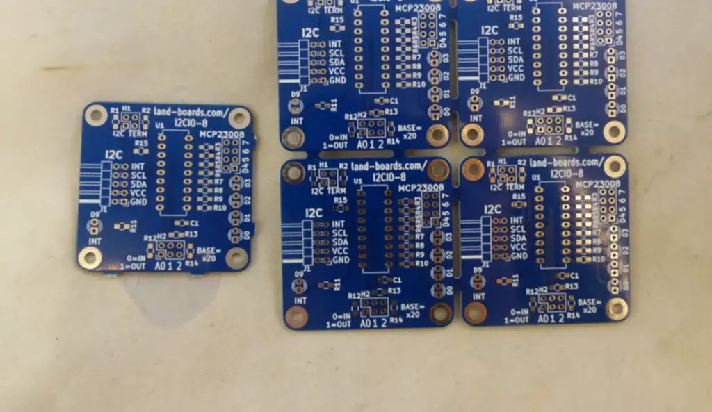
A PCB panel is a larger board that contains multiple individual PCBs arranged in a specific layout. The panel is designed to optimize the manufacturing and assembly process, reduce material waste, and improve production efficiency.
The panel is typically made of a rigid material such as FR-4 or aluminum and is designed to hold several individual PCBs. The individual PCBs are separated from each other by a routing channel, or breakaway tab, which can be easily removed after fabrication [3].
The panelization layout determines how the individual PCBs are arranged on the panel. The layout can vary depending on the size and shape of the individual PCBs and the available panel size. The goal of the layout is to optimize the use of space on the panel while minimizing waste and ensuring easy handling during fabrication and assembly.
The panelization process also involves adding fiducial marks and tooling holes to the panel. Fiducial marks are reference points that are used to align the panel during assembly, while tooling holes are used to secure the panel to the assembly equipment during fabrication.
PCB panels are commonly used in the mass production of small and medium-sized PCBs. By arranging multiple PCBs on a single panel, manufacturers can reduce overall manufacturing costs, improve production efficiency, and ensure high-quality production. The use of panels also simplifies the handling and transportation of the boards during fabrication and assembly.
Benefits of PCB Panelization:
- Reduced manufacturing costs: By grouping several individual PCBs on a single panel, manufacturers can optimize material usage and reduce overall manufacturing costs. This is because the cost of producing a single panel is generally less than the combined cost of producing multiple individual PCBs;
- Improved production efficiency: PCB panelization simplifies the handling and transportation of the boards during fabrication and assembly, which can improve overall production efficiency. The use of panels also helps to reduce the number of production steps required, which further improves efficiency;
- Minimized material waste: PCB panelization allows for the optimization of the panel layout to minimize material waste. This is because designers can efficiently utilize the available panel space and arrange the individual PCBs in a way that minimizes scrap material;
- Enhanced product quality: PCB panelization helps to ensure consistent product quality by reducing the risk of errors and defects during fabrication and assembly. This is because the use of panels provides a more stable and controlled production environment;
- Increased design flexibility: PCB panelization offers designers more flexibility in terms of board size and layout. This is because the use of panels allows for the production of larger and more complex PCB designs that may not be feasible with individual PCBs [4];
2 Major Types of Panels Used for PCB Design and Manufacturing:
Heterogeneous Composition Panels
Heterogeneous composition panels, also known as mixed-material panels, are made up of different materials, typically different types of PCB substrates. This type of panel is used when multiple PCB designs are to be assembled together but require different substrate materials for optimal performance. Heterogeneous composition panels are commonly used in applications where different PCB designs are needed for specific functions, such as RF communication or power management.
The main advantage of using heterogeneous composition panels is the ability to combine multiple PCB designs with different substrate materials into a single panel, which can significantly reduce the overall manufacturing costs. This is because the different substrates used can be selected based on the requirements of each individual design, thus reducing the cost of using more expensive substrates for all designs.
However, the use of different substrate materials can also introduce some challenges in terms of assembly and fabrication. Different substrates can have different thermal expansion coefficients, which can lead to warping and other issues during assembly. Additionally, the differences in substrate materials can also affect the quality of the plated through-holes (PTH) and can require additional processing steps to ensure a high-quality finish.
Homogenous Composition Panels
Homogeneous composition panels, on the other hand, are made up of a single substrate material, typically FR-4. This type of panel is used when multiple PCB designs require the same substrate material for optimal performance. Homogeneous composition panels are commonly used in applications where multiple PCB designs require similar electrical and mechanical properties [5].
The main advantage of using homogeneous composition panels is the ease of fabrication and assembly, as all PCB designs on the panel share the same substrate material. This can simplify the production process and reduce the risk of errors and defects during assembly. Homogeneous composition panels also tend to be more cost-effective than heterogeneous composition panels.
What Types of PCB Panel Designs Are There:
Order Panelization
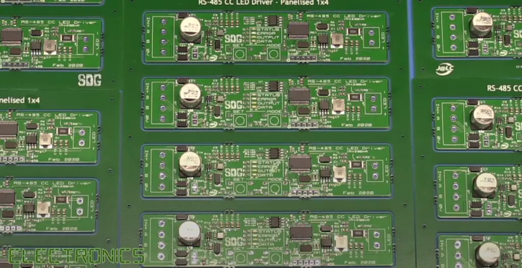
Order panelization, also known as linear panelization, is the most basic type of panelization. In this design, the PCBs are arranged in a linear fashion, side by side. The panels are typically rectangular or square in shape, with the PCBs arranged in columns and rows. This type of panelization is best suited for PCB designs that are small and have a consistent shape.
The key benefit of order panelization is simplicity. It is easy to design and manufacture, making it a popular option for low-volume production runs. However, it does have some limitations. The linear layout can lead to more wasted space on the panel, which can increase production costs. Additionally, this type of panelization is not well-suited for larger PCB designs or designs with irregular shapes.
Rotation Angle Panelization
Rotation angle panelization, also known as stepped panelization, is a type of panel design that rotates the PCBs at various angles to maximize space utilization. In this design, the PCBs are arranged in columns and rows but rotated at different angles, such as 90 degrees, 45 degrees, or 30 degrees. This allows for the PCBs to be placed closer together, reducing wasted space on the panel.
The main advantage of rotation angle panelization is its ability to maximize space utilization, which can significantly reduce production costs. This type of panelization is also well-suited for irregularly-shaped PCB designs that cannot be accommodated by order panelization. However, the angled placement of the PCBs can make it more challenging to design and manufacture, as it can affect the routing of the PCBs and require additional processing steps.
Double Side Panelization
In this design, the PCBs are typically arranged in a linear fashion on both sides of the panel. This allows for twice the number of PCBs to be produced on a single panel, reducing manufacturing costs.
The major highlight of double-side panelization is its ability to double the number of PCBs produced on a single panel, which can significantly reduce production costs. However, this type of panelization can be more challenging to design and manufacture, as it requires additional processing steps and can affect the routing of the PCBs.
Combination Panelization
This type of panelization is best suited for PCB designs that have irregular shapes or require different substrate materials for optimal performance.
The key benefit of combination panelization is its ability to optimize space utilization and reduce production costs by combining different panelization techniques. However, this type of panelization can be more complex and challenging to design and manufacture, as it requires careful consideration of the different panelization techniques and their impact on the PCB designs.
Factors of PCB Panelization Design:
1) Circuit Board Design
The circuit board design is one of the most important factors to consider when designing a PCB panelization layout. The layout of the circuit board will determine the size, shape, and orientation of the PCBs, which will impact the efficiency and effectiveness of the panelization process.
In this case, it is essential to consider the layout of the circuit board to ensure that it can be efficiently arranged on the panel. For example, if the circuit board has a rectangular shape, it may be best to use an order panelization layout. But, if the circuit board has an irregular shape, a combination panelization layout may be necessary.
2) Circuit Board Components
Another important factor to consider when designing a PCB panelization layout is the components used in the circuit board. The location and orientation of these components can impact the efficiency and effectiveness of the panelization process.
When designing a PCB panelization layout, it is important to consider the location and orientation of the components to ensure that they can be efficiently arranged on the panel. For example, if the components are all located on one side of the board, it may be best to use a double-side panelization layout. If the components are located on both sides of the board, a combination panelization layout may be necessary.
3) PCB Material
The choice of PCB material is also an important factor to consider when designing a PCB panelization layout. The type of material used will impact the size, shape, and thickness of the PCBs, which will affect the efficiency and effectiveness of the panelization process.
When designing a PCB panelization layout, it is important to consider the properties of the PCB material to ensure that it is suitable for the manufacturing process. For example, if the PCB material is too thick or rigid, it may be difficult to arrange the PCBs on the panel. Alternatively, if the PCB material is too thin or flexible, it may be difficult to process and manufacture the PCBs [6].
Top PCB Panelization Guidelines You Should Know:
Panel Size
The panel size is an important consideration when designing a PCB panelization layout. The size of the panel will impact the number of PCBs that can be arranged on the panel and the overall efficiency of the panelization process.
It is important to choose a panel size that maximizes the number of PCBs that can be arranged on the panel while still allowing for proper tooling and handling. A larger panel size may be more efficient in terms of manufacturing, but it may also increase the risk of damage during handling and shipping.
Layer Stackup
The layer stack up is the arrangement of the copper layers and dielectric layers that make up the PCB. It is a key consideration when designing a PCB panelization layout, as it will impact the overall thickness and rigidity of the panel.
When arranging PCBs on a panel, it is important to ensure that the layer stack up is consistent across all the PCBs. This will ensure that the panel is uniform and that there are no issues with component clearance or assembly.
Panel Structure
To maximize the number of PCBs that can be arranged on the panel while still ensuring that the panel is easy to handle and process.
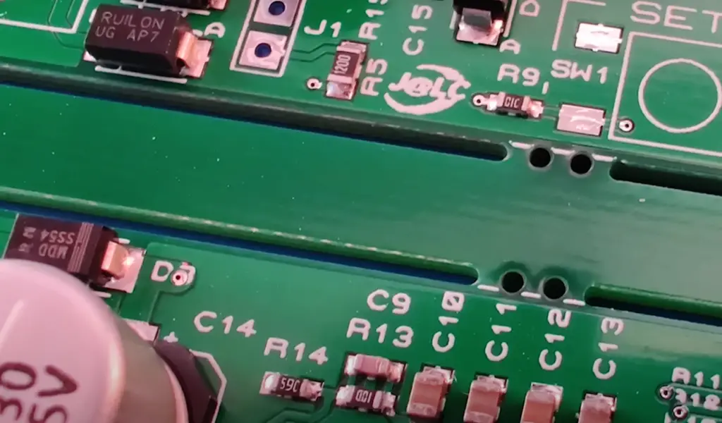
When designing the panel structure, it is important to consider the spacing between the PCBs, as well as the location and size of the breakouts and tooling holes. These features must be carefully designed to ensure that they do not interfere with the PCBs or the manufacturing process.
Panel Layout
The panel layout is the arrangement of the PCBs on the panel. It is essential to carefully plan the panel layout to ensure that the PCBs are arranged in an efficient and effective manner.
When arranging the PCBs on the panel, it is important to consider the orientation of the components and the routing of the traces. This will ensure that the PCBs can be easily assembled and that there are no issues with component clearance or assembly [7].
Breakouts
It is important to carefully design the breakouts to ensure that they are clean and uniform and that they do not damage the PCBs during the separation process.
When designing the breakouts, it is important to consider the thickness and rigidity of the panel, as well as the location and size of the breakouts. The breakouts must be designed to ensure that they do not interfere with the PCBs or the manufacturing process.
Component Clearances
The component clearances are the spaces between the components on the PCB. It is important to ensure that there is sufficient clearance between the components to allow for proper assembly and operation.
When designing the panel layout, it is important to consider the location and orientation of the components, as well as the size and shape of the PCB. This will ensure that the component clearances are sufficient and that there are no issues with assembly or operation.
Panel Tooling
The panel tooling refers to the holes and slots on the panel that are used to secure the panel during the manufacturing process. It is important to carefully design the panel tooling to ensure that the panel is secure and easy to handle during processing.
When designing the panel tooling, it is essential to consider the size and location of the tooling holes, as well as the spacing between them. This will ensure that the panel is held securely in place during processing and that there are no issues with damage or misalignment.
Additionally, it is important to consider the type of tooling that will be used, such as pins, clips, or vacuum holes. The type of tooling will impact the efficiency and accuracy of the manufacturing process, so it is important to choose the right type of tooling for the specific application.
Should PCB Designers Layout Their Own Panels?
In general, PCB designers should leave the panelization process to an experienced supplier or engineer. This is because a successful panel design requires knowledge of production processes and materials as well as efficient use of space. The layout must also be optimized for cost efficiency. Having an expert create the design can save time, and money and help prevent costly mistakes due to inexperience.
Additionally, if the board designer does not have experience in the field of panelization, then any designs they make may not work out correctly when put into production. Designers should ensure that their individual boards are properly designed before attempting to panelize them on their own.
If you do decide to take on your own panelization project, there are a few factors to consider. You should be familiar with the manufacturing requirements and processes, such as machine compatibility and panel size restrictions. Be sure to also take into account any sheet material constraints and design rules that might affect your panel’s production. Additionally, you should have an understanding of board-to-board orientation for efficient routing paths, as well as spacing considerations for both via holes and components.
Ultimately, creating a successful PCB panel requires expertise in both the design side of things as well as knowledge about materials and processes used during production. Unless the designer is experienced with the entire process from start to finish, it is usually best to leave this job to professionals. Doing so can help ensure cost efficiency, quality performance, and on-time delivery of your boards.
One final note – if you do decide to layout the panel yourself, make sure to review it with an expert before sending it off for manufacturing. This can help prevent costly mistakes and ensure that your PCB panels are produced correctly and quickly when they reach the factory
Understand PCB Panelization Design Guidelines:
1) PCB Panelization Design Method:
- V-Score Panelization involves creating a groove or a V-shaped cut on the board, which can be broken off manually or with the help of a machine. The score lines are cut into the board’s top layer, while the bottom layer is left intact. The V-Score panelization method allows PCBs to be easily separated from a larger panel without any stress on the components;
- Solid Tab Panelization involves creating small tabs that hold the individual PCBs in place on a larger panel. The tabs are then broken off once the manufacturing process is complete. Solid Tab panelization is best suited for PCBs with sensitive components or where there is a need for a high degree of accuracy during the manufacturing process [8];
2) Matters Needing Attention in PCB Panelization Design:
- Gap: A minimum gap of 2mm is recommended between each PCB on the panel. This allows for easy handling during the manufacturing process and ensures that there is enough clearance for any cutting or scoring processes that may be involved;
- Label Placement Problem: Labels are an essential part of any PCB design. They help identify the board’s components, and their placement on the board should be carefully considered during panelization. The labels should be placed in such a way that they do not interfere with the manufacturing process, and they are not covered by any cutting or scoring lines;
- The Location of The Perforation: The location of the perforation should be considered during panelization. If the perforation is too close to any critical components, it may cause damage to the board during separation;
- PCB Array Arrangement: The arrangement of the PCB array on the panel should be considered to ensure that the manufacturing process is carried out efficiently. The spacing between the PCBs should be consistent to avoid any interference during the separation process;
3) PCB Panelization Design – Problems That Are Easy to Appear in the PCB Array:
- Manually Breaking Tabs: Breaking tabs manually can lead to uneven separation, which may cause damage to the components on the board;
- Breaking with A Machine: Breaking tabs with a machine can lead to stress on the board and may cause damage to the components;
- Manually Breaking V-Grooves: Manually breaking V-Grooves can lead to uneven separation and may cause damage to the components on the board;
- Cutting V-Grooves: Cutting V-Grooves can lead to stress on the board, which may cause damage to the components;
4) PCB Panelization Design – Panel Wiring Method:
- Circuit Board Shape: The shape of the circuit board should be considered during panelization. The shape should be optimized for ease of manufacturing, and the panel should be designed in such a way that it minimizes waste;
- Edge Components: Components located at the edge of the board should be carefully considered during panelization. The placement of these components can affect the ease of manufacturing, and may require additional support or clearance;
- Edge Quality: The quality of the edges of the PCBs on the panel is crucial. The edges must be smooth to avoid any damage to the components during the separation process;
- Time Spent: The time spent during the panelization process should be optimized to improve efficiency and reduce costs. The panelization design should be created in a way that minimizes the time required for separation and assembly;
- Waste of Materials: Material waste can be a significant issue during the panelization process. The panel design should be optimized to minimize waste and reduce costs [9];
Other Considerations for PCB Panelization Design
- Quality Control: Quality control is essential during the panelization process. Proper quality control measures should be in place to ensure that the panelization design meets the required standards and specifications;
- Safety Considerations: Safety should be a top priority during the panelization process. Proper safety measures should be in place to ensure that the manufacturing process is carried out safely and efficiently;
FAQ
1. What software is used for PCB panelization?
There are various software tools available for PCB panelization, including popular CAD software such as Altium, Eagle, and KiCad. Additionally, some PCB manufacturers provide their own panelization software that can be used to create and optimize PCB panel layouts [10].
2. How to design a PCB panel?
Designing a PCB panel involves arranging multiple PCBs onto a larger panel that can be manufactured in a single production run. This can be done manually or with the help of panelization software. The process involves determining the orientation and spacing of the individual PCBs, adding support rails or breakaway tabs to ensure stability during manufacturing, and specifying fiducial marks to aid in alignment and inspection.
3. What is a PCB panel array?
The individual PCBs are spaced and oriented according to the manufacturer’s specifications, and additional features such as breakaway tabs and fiducial marks may be included.
4. What are the types of PCB panels?
PCB panels can be categorized by their layout or configuration, such as single-panel or multi-panel layouts, rectangular or irregular shapes, and panelization with or without support rails or breakaway tabs. Additionally, the type of PCB material, thickness, and finish can affect the layout and configuration of the panel.
5. What is a typical PCB panel?
A typical PCB panel may consist of multiple individual PCBs arranged in a regular or irregular layout with support rails or breakaway tabs. The individual PCBs may have different designs or be identical and may include fiducial marks for alignment and inspection.
6. What material is a PCB panel?
PCB panels are typically made of the same materials as individual PCBs, such as FR-4 fiberglass composite or other materials specified by the manufacturer.
7. What is the standard PCB panel size?
There is no single standard PCB panel size, as manufacturers may offer different sizes and configurations depending on their equipment and capabilities. However, common panel sizes include 18″ x 24″ or 21″ x 24″, and custom sizes may be available upon request [11].
8. Why is PCB so expensive?
PCBs can be expensive due to several factors, including the complexity and density of the design, the number of layers, the type of material used, the size and quantity of the order, and the manufacturer’s capabilities and equipment. Additionally, specialized finishes or coatings, such as gold plating, can add to the cost.
9. Which tool is best for PCB design?
The best tool for PCB design depends on the individual’s needs and preferences, as well as the complexity and requirements of the design. Popular options include Altium, Eagle, and KiCad, as well as other proprietary or open-source software tools.
10. What is 4 layer PCB design rule?
The 4-layer PCB design rule refers to the minimum number of layers required for a specific type of PCB design. A 4-layer PCB includes two inner layers sandwiched between two outer layers, which provides more space for routing traces and power and ground planes.
11. What is the maximum PCB panel size?
The maximum PCB panel size depends on the equipment and capabilities of the manufacturer. Common sizes range from 18″ x 24″ to 21″ x 24″, but custom sizes may be available upon request [12].
12. How thick is a PCB panel?
The thickness of a PCB panel depends on the specific materials and design specifications. Common thicknesses range from 0.031″ to 0.062″, but other thicknesses may be available [13].
13. What are 5 examples of types of PCB testing methods?
Examples of PCB testing methods include:
- Visual inspection involves examining the PCB for any physical defects or abnormalities, such as broken traces, missing components, or misaligned parts;
- Electrical testing involves verifying that the circuit functions correctly by applying a test signal and measuring the response;
- X-ray inspection can be used to inspect the inner layers of a multilayer PCB, allowing for the detection of any defects or issues that may not be visible through visual inspection;
- In-circuit testing involves testing each component on the PCB individually to verify that it functions correctly;
- Functional testing involves verifying that the PCB performs as expected in a real-world application;
14. What is the difference between a PV module and a panel?
A PV module, also known as a solar panel, is a collection of individual solar cells that are connected together to form a larger unit that generates electricity from sunlight. A PV panel, on the other hand, is a collection of multiple PV modules that are mounted together to form a larger unit. While both PV modules and panels use solar cells to generate electricity, a panel consists of multiple modules and is designed to generate more power than a single module.
15. How many PCBs are in a panel?
The number of PCBs in a panel can vary depending on the manufacturer’s capabilities and the design requirements. Common panel configurations include 2-up, 4-up, 6-up, 8-up, and 10-up, which correspond to the number of identical PCBs arranged in a single panel.
Useful Video: Manual panelizing of PCBs with tabs and mouse bites
References
- https://www.lpkf.com/en/pcb-design-guidelines
- https://resources.pcb.cadence.com/blog/2021-pcb-panelization-guidelines-for-layout-considerations
- https://www.electronicdesign.com/technologies/boards/article/21801451/pcb-designers-need-to-know-these-panelization-guidelines
- https://www.mclpcb.com/blog/pcb-panelization-guidelines/
- https://madpcb.com/pcb-panelization-guidelines/
- https://jhdpcb.com/pcb-panelization/
- https://www.mktpcb.com/assembly/pcb-panelization/
- https://www.wevolver.com/article/pcb-panelization-everything-you-need-to-know
- https://www.rigiflex.com/blog/a-brief-guide-to-pcb-panelization-and-pcb-panel-guidelines/
- https://www.vse.com/blog/2020/11/05/eight-important-pcb-panelization-guidelines-to-know/
- https://www.wellpcb.com/pcb-panelization-design.html
- https://www.pentalogix.com/blog/2023/01/11/what-is-pcb-panelization
- https://www.tempoautomation.com/blog/what-is-the-standard-pcb-thickness/