Printed circuit board (PCB) design is a crucial aspect of electronics engineering. It involves creating a layout of electronic components and their interconnections on a PCB. This layout must be optimized to ensure the reliable and efficient operation of the circuit.
PCB design rules are a set of guidelines that define the minimum and maximum values for various parameters that affect the performance and manufacturability of the PCB. These rules are essential for achieving a functional and reliable PCB design [1].
PCB design rules cover a range of parameters, including trace width and spacing, via sizes, pad sizes, drill sizes, and placement rules. These rules must be followed to ensure that the PCB can be manufactured correctly, without errors or defects.
For example, trace width and spacing rules ensure that the copper traces on the PCB can carry the required current without overheating or causing electromagnetic interference (EMI). Via and pad size rules ensure that the PCB can be assembled and soldered correctly, and drill size rules ensure that the vias and through holes can be drilled accurately.
In this article, we will explore the PCB design rules and give certain recommendations to beginners.
Difference Between Analog And Digital PCBs
Analog and digital PCBs (Printed Circuit Boards) differ in terms of their circuit design and layout considerations.

Analog circuits use continuous variables, such as voltages or currents that vary in a smooth and linear manner. In contrast, digital circuits use binary variables, such as high or low voltages, corresponding to logical values of 1 or 0 [2].
Analog PCBs require great attention to detail as they are more sensitive to noise and require low tolerance levels. The layout of an analog PCB must consider shielding, grounding, and impedance matching, among other factors. On the other hand, digital PCBs operate at higher frequencies but are less sensitive to noise. The design of digital PCBs focuses on controlling signal integrity, reducing transmission line effects, and minimizing ground bounce.
These signals are represented by varying voltage or current levels that change over time, and the PCB must be designed to maintain the signal’s integrity by minimizing noise and distortion. Analog PCBs typically have fewer components than digital PCBs and require higher precision in their design and manufacturing to ensure proper signal processing and transmission.
On the other hand, digital PCBs are designed to process and transmit discrete signals, such as binary code. These signals are represented by two states, high or low voltage, and the PCB must be designed to ensure that these states are maintained accurately. Digital PCBs require more components than analog PCBs, such as logic gates and memory elements, and must be designed with specific timing requirements to ensure proper functioning.
In terms of functionality, analog PCBs are commonly used in audio equipment, radio receivers, and other devices that process continuous signals. Digital PCBs, on the other hand, are used in computers, digital cameras, and other devices that process discrete signals.
The applications of analog and digital PCBs also differ in terms of their power consumption and noise levels. Analog PCBs typically consume less power than digital PCBs because they do not require high-speed switching, which generates noise and consumes more power. However, analog PCBs are more susceptible to noise, which can cause distortion in the signal. Digital PCBs, on the other hand, consume more power but are less susceptible to noise.
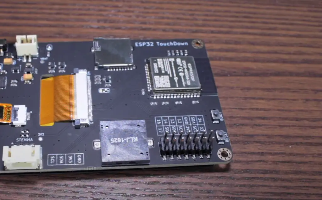
Criteria For Selection of PCB Materials for Digital Circuits:
- Dielectric constant: This is a measure of how well a material stores electrical energy in an electric field. Lower dielectric constants are generally better for high-speed digital circuits, as they reduce signal distortion and loss;
- Loss tangent: This is a measure of how much of the electrical energy stored in the dielectric is lost as heat. Lower loss tangents are better for high-speed digital circuits, as they reduce signal attenuation and distortion;
- Copper foil: High-quality copper foil with a high level of purity and a low profile can minimize signal losses and ensure reliable signal transmission in high-speed digital circuits;
- Thermal conductivity: Good thermal conductivity can help dissipate heat generated by high-speed digital circuits;
- Glass transition temperature: The glass transition temperature is the temperature at which a material transitions from a hard, brittle state to a more flexible, rubbery state. For digital PCBs, it is important to choose materials with a high glass transition temperature to prevent warping or damage to the circuit at high temperatures [3];
PCB Design Layout Guidelines for Engineers:
1) Before the Layout Starts
Before starting the PCB design layout, it is important to establish a clear understanding of the requirements and constraints of the project. This includes the electrical requirements of the circuit, the mechanical requirements of the board, the available space for the board, and the manufacturing process.

Once these requirements have been established, the following PCB design layout guidelines should be followed:
- Libraries. The libraries are a critical component of the PCB design layout process. The libraries contain the schematic symbols and footprints for each component that is used in the circuit. It is important to ensure that the libraries used are up-to-date and accurate. If a library does not contain a specific component, it should be created or imported from a reliable source. The accuracy of the libraries directly impacts the accuracy of the PCB design layout;
- Board Outline and Layer Stackups. The board outline and layer stack-ups are the physical dimensions and layer configurations of the PCB. The board outline determines the physical size and shape of the board, while the layer stack-up determines the number and order of the layers in the board. The board outline and layer stack-ups should be carefully planned to meet the mechanical and electrical requirements of the circuit;
- CAD Parameters and Settings. The CAD parameters and settings should be set up correctly before starting the PCB design layout. This includes the units of measurement, grid size, and snap settings. The parameters and settings should be consistent with the requirements of the project;
2) Guidelines for Placing PCB Components
Once the libraries, board outline, layer stack-ups, and CAD parameters and settings have been established, the next step is to place the components on the board.
The following PCB design layout guidelines should be followed when placing components:
- Circuit Performance. The placement of the components directly affects the performance of the circuit. Components that interact with each other should be placed close together to reduce the length of the traces and the potential for interference. Components that generate heat should be placed in locations that allow for adequate cooling. The placement of components should be optimized for the best circuit performance;
- Manufacturability. The placement of components should also consider the manufacturing process. Components that are difficult to place or solder should be avoided, if possible. Components should be placed in a manner that allows for easy access during the assembly process. The placement of components should be optimized for the ease of manufacturing;
- Accessibility. The placement of components should also consider the accessibility of the board. Components that require adjustment or replacement should be placed in locations that are easy to access. The placement of components should be optimized for ease of maintenance;
3) PCB Design Layout Guidelines for Routing:
Design Rules and Constraints
The design rules and constraints should be set up before routing the PCB. The design rules and constraints should be consistent with the requirements of the project and the capabilities of the manufacturing process.

Signal and Power Integrity
Signal and power integrity are critical factors in the performance of a PCB. Signal integrity refers to the quality of the signal as it travels through the traces and vias of the PCB. Power integrity refers to the ability of the power supply to deliver stable and clean power to the components.
The following PCB design layout guidelines should be followed to ensure signal and power integrity:
- Trace length matching is the process of ensuring that the traces that carry the same signal have the same length. This is important to prevent timing issues that can affect the performance of the circuit. Trace length matching should be done for high-speed signals;
- Impedance matching is the process of ensuring that the impedance of the trace matches the impedance of the source and the load. This is important to prevent reflections and signal distortions. Impedance matching should be done for high-frequency signals;
- Ground and power planes are important for signal and power integrity. Ground planes provide a stable reference voltage for the signals, while power planes provide a stable source of power for the components. The ground and power planes should be placed close to the signal traces to reduce the impedance and the potential for interference;
- Via placement is important for signal and power integrity. Vias should be placed in locations that do not interfere with the signal or power traces. Vias should also be placed in locations that allow for easy manufacturing [4];
“Golden” Rules Of PCB Design:
Fine-Tune Component Placement
One of the most important aspects of PCB design is component placement. The placement of components on a PCB can have a significant impact on the performance and reliability of the circuit. It is important to carefully consider the placement of each component to ensure that it is in the optimal location for its intended function. This involves taking into account factors such as signal integrity, thermal management, and ease of assembly and testing.
When placing components on a PCB, it is important to avoid placing them too close together or too far apart. Components that are too close together can interfere with each other’s signals, while those that are too far apart can lead to long signal paths and increased noise. It is also important to consider the orientation of components, particularly those that are polarized or have specific pinouts.

Power, Ground & Signal Traces
Another critical aspect of PCB design is trace routing. The routing of traces on a PCB can have a significant impact on the performance and reliability of the circuit. It is important to carefully consider the routing of power, ground, and signal traces to ensure that they are optimized for their intended function.
Power and ground traces should be routed first, as they form the backbone of the circuit. These traces should be as wide as possible to minimize resistance and minimize voltage drop. Signal traces should be routed after the power and ground traces have been routed, and should be kept as short as possible to minimize noise and signal loss.
Keep Things Separate
One of the key principles of PCB design is to keep things separate. This means separating power and ground planes, as well as separating analog and digital signals. Separating these elements helps to minimize interference and noise, and improves signal integrity.
In addition to separating power and ground planes and analog and digital signals, it is also important to separate high-speed and low-speed signals. High-speed signals should be routed on their own layer, with a dedicated return path, to minimize noise and signal loss.
Minimize Heating Issues
Heating is a common problem in PCB design, particularly in high-power applications. To minimize heating issues, it is important to carefully consider the thermal management of the circuit. This involves selecting the appropriate components and materials, as well as optimizing the layout and routing of the PCB.
Components that generate heat, such as power amplifiers and voltage regulators, should be located away from sensitive components to minimize the impact of heat. In addition, it is important to use thermal vias to transfer heat away from the components and to dissipate heat through the PCB.
Verify Your Layout Against Your PCB Design Rules
Before finalizing your PCB layout, it is important to verify that it meets your design rules. This involves performing a Design Rule Check (DRC) to ensure that the layout complies with your specified parameters. This can help to identify any potential issues, such as clearance violations or trace width violations before the PCB is manufactured.
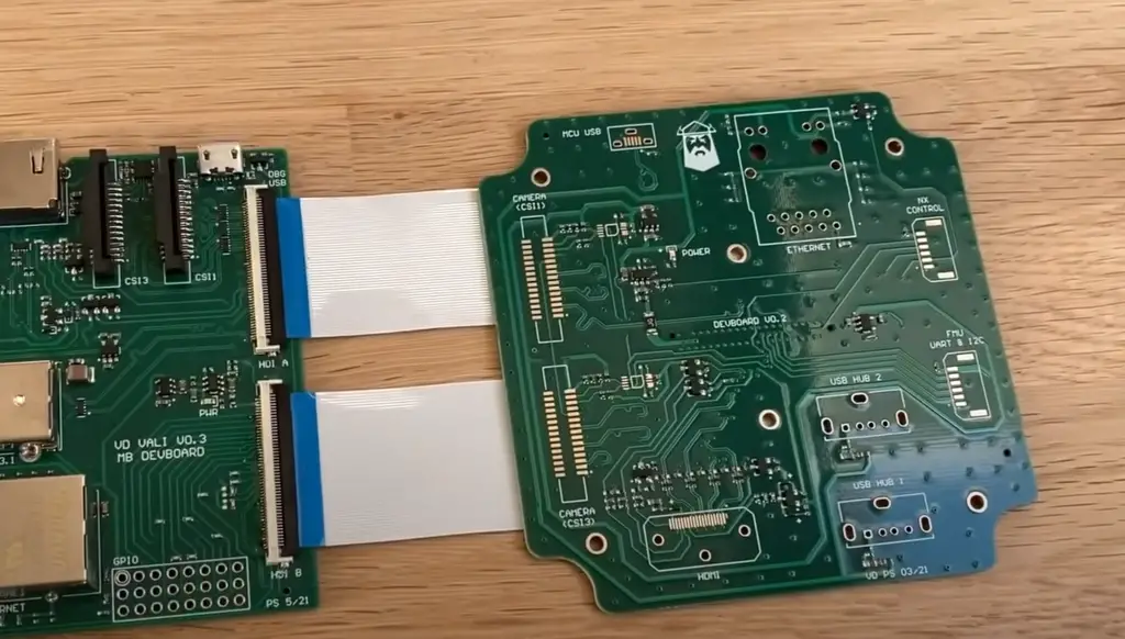
Choose The Right Grid-Set
When designing a PCB, it is important to select the appropriate grid set. The grid set determines the spacing between components, traces, and vias, and can have a significant impact on the layout and routing of the PCB. The grid set should be selected based on the size and spacing of the components, as well as the minimum trace and via width.
Always Use the Grid Spacing That Matches the Most Components
One of the most crucial aspects of PCB design is component placement. The placement of components affects the performance, reliability, and manufacturability of a PCB. To ensure that components are correctly placed on the board, engineers use a grid system. The grid system is a set of vertical and horizontal lines that define the placement of components on the PCB.
When designing a PCB, it is essential to use a grid spacing that matches most components. This helps to ensure that components are placed uniformly on the board, which can improve the overall aesthetics and manufacturability of the PCB. Using a grid spacing that matches most components also helps to ensure that components are aligned correctly, which can improve the reliability of the PCB.
Keep the Path the Shortest and Most Direct
The path of a trace on a PCB can significantly affect the performance of the circuit.
When routing traces on a PCB, engineers must consider various factors, such as signal frequency, impedance, and crosstalk. High-frequency signals require shorter and more direct traces to minimize noise and signal degradation. Traces that carry high-current signals also require shorter and wider traces to reduce resistance and heating issues.
Use the Power Layer as Much as Possible
The power and ground planes on a PCB are critical for providing a stable voltage and reference potential for the circuit. Using the power layer as much as possible can help to reduce the overall resistance of the circuit, which can improve the reliability and efficiency of the PCB. When designing a PCB, it is essential to ensure that the power layer is properly connected to the components and ground plane.

Group Related Components Together with the Required Test Points
Grouping related components together can help to reduce the overall size of the PCB and improve the performance of the circuit. By placing related components together, engineers can reduce the length of traces, which can minimize signal degradation and noise. Grouping related components also help to improve the accessibility of the test points, which can simplify testing and debugging [5].
Copy the Required Circuit Board on Another Larger Circuit Board Multiple Times
Copying the required circuit board on another larger circuit board multiple times can help to simplify the design and manufacturing process. By using the same design for multiple circuit boards, engineers can reduce the overall cost and time required for manufacturing. This approach is commonly used in the mass production of electronic devices.
Integrate Component Values
Integrating component values can help to simplify the design process and improve the reliability of the PCB. By integrating component values, engineers can reduce the number of components and traces on the board, which can simplify testing and reduce the overall cost of the PCB. Integrating component values can also improve the reliability of the PCB by reducing the number of potential failure points.
Perform Design Rule Checks (DRC) As Much As Possible
Performing Design Rule Checks (DRC) is an important step in the PCB design process. This involves using software tools to check the design against a set of predefined rules to ensure that it meets certain criteria for manufacturability and functionality.
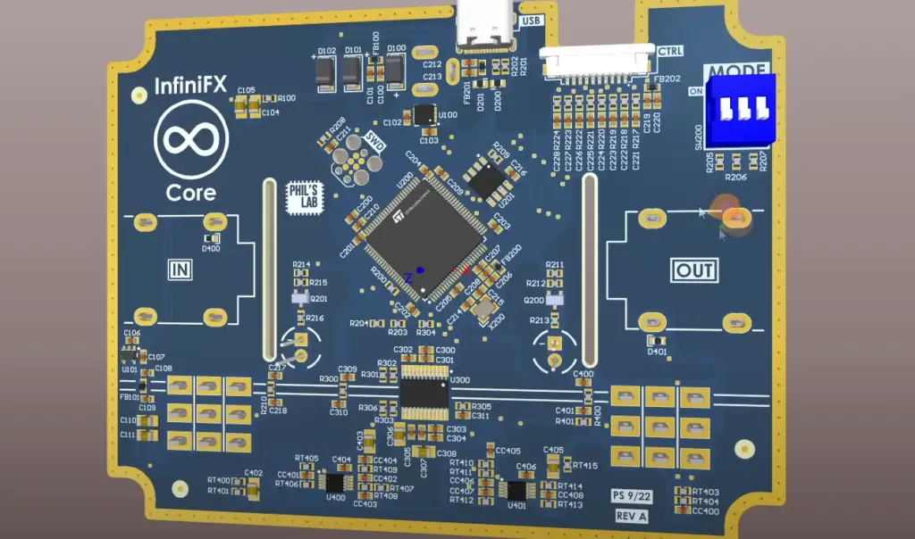
The first step in performing a DRC is to define the rules that need to be checked. This involves setting up parameters such as minimum trace widths and clearances, drill sizes, and board thickness. Once these rules are defined, the software tool can perform a check on the design to ensure that it meets these requirements.
Some of the most common DRC checks include:
- Clearance checks: This involves checking the distance between different components, traces, and pads to ensure that they are not too close together, which could cause short circuits;
- Trace width checks: This involves checking the width of the traces to ensure that they are wide enough to carry the required current without overheating;
- Drill size checks: This involves checking the size of the holes drilled in the board to ensure that they are large enough to accommodate the components and pins;
- Solder mask checks: This involves checking the areas where the solder mask is applied to ensure that there are no gaps or overlaps that could cause solder bridges or other issues during assembly;
Performing DRC checks early in the design process can save a lot of time and money by identifying potential issues before the board is manufactured. It also ensures that the board is designed to meet the required specifications and standards, which is important for ensuring its functionality and reliability.
Use Screen Printing Flexible
It’s an essential aspect of the PCB design process because it allows designers to convey important information such as component identifiers, polarity, and reference designators.
When designing a PCB, it’s essential to use screen printing efficiently to maximize its benefits. For example, it’s a good practice to include reference designators on the silkscreen layer, indicating the component location and identification number. It’s also advisable to use unique shapes and colors for different types of components, making them easier to identify.
However, screen printing has limitations that designers need to consider. The resolution of the printing process can affect the readability of the text, symbols, and logos on the PCB surface. Therefore, it’s essential to ensure that the screen printing is legible and meets the minimum line width and height requirements specified in the PCB design rules.
Decoupling Capacitors Must Be Selected
Decoupling capacitors play a critical role in PCB design by reducing noise and ensuring stable power delivery to the components. They are placed in parallel with the power supply pins of integrated circuits to filter out high-frequency noise and prevent voltage drops during transient events.
When selecting decoupling capacitors, designers must consider their capacitance and voltage rating. The capacitance of the capacitor should be large enough to filter out the high-frequency noise, but not too large to cause unwanted resonances. The voltage rating should be higher than the maximum voltage that the capacitor will experience during operation [6].

It’s also essential to place the decoupling capacitors as close as possible to the power supply pins of the integrated circuits. This reduces the inductance of the connection between the capacitor and the integrated circuit, ensuring optimal noise reduction and power delivery.
Generate PCB Manufacturing Parameters and Verify Them
Once the PCB design is complete, designers need to generate the manufacturing parameters required to produce the PCB. This involves generating the Gerber files, drill files, and bill of materials (BOM) required by the PCB manufacturer.
Designers need to verify the generated files against the PCB design rules to ensure that they are accurate and meet the manufacturing requirements. This involves checking the minimum track width and clearance, drill sizes, and placement accuracy, among other factors.
It’s also essential to communicate with the PCB manufacturer and clarify any discrepancies in the manufacturing parameters. This ensures that the PCB is manufactured to the desired specifications and reduces the likelihood of production errors.
Where to Place Power and Ground Planes?
Power and ground planes are essential aspects of PCB design. They provide a low-impedance path for the flow of current and ensure stable power delivery to the components.
When placing power and ground planes, designers need to consider their location and configuration. The power and ground planes should be placed adjacent to each other to minimize the loop area and reduce electromagnetic interference (EMI).
It’s also essential to avoid splitting the power and ground planes into multiple sections as this can cause ground loops and EMI. In addition, designers need to ensure that the power and ground planes are adequately connected to each other using multiple vias to reduce impedance.
Finally, designers need to ensure that the power and ground planes are not too close to high-speed signal traces as this can cause unwanted coupling and noise. It’s essential to maintain a minimum distance between the signal traces and the power and ground planes to reduce coupling and ensure signal integrity.
FAQ
1. What is silkscreen testing?
This ink layer is called the silkscreen layer and is used to print component labels, reference designators, logos, and other graphics on the PCB. Silkscreen testing involves verifying that the silkscreen layer is correctly aligned with the PCB’s other layers and that the ink is applied evenly and accurately. Silkscreen testing is an essential step in ensuring that the PCB is correctly assembled and labeled.
2. What are the rules of thumb for PCB design?
There are several rules of thumb for PCB design that can help ensure the reliability and functionality of the PCB [7].
Some of the most common rules of thumb include:
- Maintaining uniform trace width and spacing;
- Minimizing the use of vias;
- Keeping high-speed signals short and direct;
- Avoiding sharp angles in the trace routing;
- Keeping sensitive components away from noisy components;
Other design considerations include choosing appropriate layer stack-up, trace thickness, and pad sizes. The specific design rules of thumb will depend on the PCB’s application and the manufacturing process used.
3. What are PCB standards?
PCB standards are guidelines or specifications that define the requirements for PCB manufacturing and design. These standards are developed and maintained by organizations such as the International Electrotechnical Commission (IEC), the Institute of Electrical and Electronics Engineers (IEEE), and the International Organization for Standardization (ISO). PCB standards cover a range of topics, including PCB materials, manufacturing processes, design rules, and environmental requirements [8].
4. What is the ISO standard for PCB?
The ISO standard for PCB is ISO 10474, which covers the inspection and testing of PCBs. This standard outlines the requirements for the testing and inspection of PCBs to ensure that they meet the required specifications and are suitable for their intended use. ISO 10474 covers the visual, dimensional, electrical, and mechanical inspection of PCBs and provides guidance on how to perform these tests [9].
5. How do you calculate PCB size?
PCB size is typically calculated based on the size of the components and the required routing space. To calculate the PCB size, you will need to consider the size and placement of the largest components, the required trace routing space, the number of layers, and the overall board shape. The PCB size should be chosen to provide adequate spacing for the components and routing while minimizing the board’s overall size and cost.
6. How do I choose PCB thickness?
The choice of PCB thickness depends on several factors, including the mechanical strength required, the number of layers, the type of components used, and the manufacturing process used. Thicker PCBs are generally more robust and can handle higher loads, while thinner PCBs are more flexible and can be used in applications where space is limited. The specific PCB thickness should be chosen based on the application’s requirements and the manufacturing process used.
7. What is the minimum PCB thickness?
The minimum PCB thickness depends on the manufacturing process used and the PCB’s application. For example, the minimum thickness for a single-sided PCB is typically around 0.4mm, while the minimum thickness for a multilayer PCB can be as low as 0.2mm. Thinner PCBs can be more challenging to manufacture and may have limitations on the type of components that can be used [10].
8. What is the most common issue in designing PCB?
One of the most common issues in designing PCBs is errors in the layout or routing. These errors can include incorrect trace widths, inadequate spacing between traces, and incorrect placement of components.
Other common issues include noise and interference, power supply issues, and thermal management. To avoid these issues, it is essential to follow design rules of thumb, perform thorough testing and verification, and work closely with the PCB manufacturer to ensure that the design is suitable for the manufacturing process.
9. What is PCB material called?
The PCB material is typically made of a non-conductive substrate that is coated with a thin layer of conductive material. The substrate can be made of various materials, including fiberglass, epoxy resin, and polyimide. The conductive material is usually copper and is used to create the traces and pads on the PCB.
The combination of the substrate and conductive material is often referred to as PCB laminate. Different types of laminates are available, and the choice will depend on the specific requirements of the application, including mechanical strength, thermal management, and signal integrity.
10. What are the 3 types of PCB?
3 main types of PCBs are single-sided PCBs, double-sided PCBs, and multi-layer PCBs:
- Single-sided PCBs have components and traces on one side of the board and are the simplest and most cost-effective type of PCB;
- Double-sided PCBs have components and traces on both sides of the board, allowing for more complex circuits;
- Multi-layer PCBs have multiple layers of conductive material and insulation, allowing for even more complex circuits and higher component density;
11. What is PCB frequency?
The PCB frequency depends on various factors, including the thickness and material of the PCB, the type of components used, and the manufacturing process used. PCB designers and manufacturers need to consider the frequency requirements of the application and ensure that the PCB is designed and manufactured to meet those requirements.
12. How thick is a 20-layer PCB?
The thickness of a 20-layer PCB can vary depending on the materials and manufacturing process used. Generally, the total thickness of a 20-layer PCB can range from 1.0 mm to 3.0 mm, with each layer being approximately 0.05 mm to 0.2 mm thick [11].
13. What are PCB design basics?
PCB design basics involve understanding the fundamentals of designing a printed circuit board, including component placement, routing, and layer stack-up. The basics of PCB design also include understanding design rules of thumb, such as trace width and spacing, via placement, and power and ground planes. Designing a PCB involves considering the application requirements, selecting the appropriate components, and optimizing the design for manufacturability and reliability.
14. What is PCB quality?
PCB quality refers to the level of excellence in the design, manufacturing, and testing of a printed circuit board. A high-quality PCB meets the required specifications, functions reliably, and has a long lifespan. PCB quality involves ensuring that the design is optimized for manufacturability, selecting appropriate materials and components, following quality control processes during manufacturing, and performing thorough testing and verification.
15. What causes PCB failure?
PCB failure can be caused by various factors, including manufacturing defects, design errors, environmental factors, and component failures. Manufacturing defects can include issues such as poor soldering or contamination, which can lead to short circuits or open circuits. Design errors can result in issues such as noise and interference or inadequate thermal management. Environmental factors such as temperature, humidity, and vibration can also cause PCB failure over time.
16. What is the maximum PCB size?
The maximum PCB size is determined by various factors, including the manufacturing process used and the capabilities of the manufacturer. The maximum PCB size can range from a few square millimeters to several square meters, depending on the application and the manufacturing process used.
17. How do I choose PCB thickness?
Choosing the appropriate PCB thickness involves considering the mechanical strength required, the number of layers, the type of components used, and the manufacturing process used. Thicker PCBs are generally more robust and can handle higher loads, while thinner PCBs are more flexible and can be used in applications where space is limited. The specific PCB thickness should be chosen based on the application’s requirements and the manufacturing process used.
18. How do you calculate the PCB layer?
The number of layers in a PCB is determined by the complexity of the circuit and the required routing space. To calculate the number of layers, you will need to consider the number of components, the size and placement of the components, the required trace routing space, and the overall board shape. Generally, as the complexity of the circuit increases, the number of layers required also increases.
19. What is the PCB life cycle?
The PCB life cycle refers to the stages of a printed circuit board, from the initial design and prototyping phase to end-of-life disposal. The PCB life cycle includes various stages: design and development, manufacturing, assembly, testing and validation, distribution, and end-of-life disposal. During the life cycle of a PCB, various factors can impact the reliability and performance of the board, including environmental factors, component aging, and wear and tear. Proper design, manufacturing, and testing processes can help to extend the PCB’s life cycle and ensure that it functions reliably throughout its intended use.
Useful Video: PCB Design – Getting Started & Design Rules
References
- https://resources.altium.com/p/pcb-layout-guidelines
- https://www.pcbcart.com/article/content/rules-of-PCB-design.html
- https://www.raypcb.com/13-basic-rules-of-pcb-layout/
- https://resources.pcb.cadence.com/blog/2021-pcb-design-layout-guidelines-for-engineers
- https://resources.pcb.cadence.com/blog/2021-some-key-design-rules-for-pcb-layout
- https://www.optimatech.net/knowledge-center/pcb-design-guidelines.aspx
- https://www.7pcb.com/blog/pcb-design-rules
- https://www.eurocircuits.com/pcb-design-guidelines/
- https://www.electronics-notes.com/articles/analogue_circuits/pcb-design/pcb-design-layout-guidelines.php
- https://www.ncabgroup.com/pcb-design-guidelines/
- https://www.proto-electronics.com/blog/the-top-5-rules-for-digital-pcb-design




Leave a Reply