
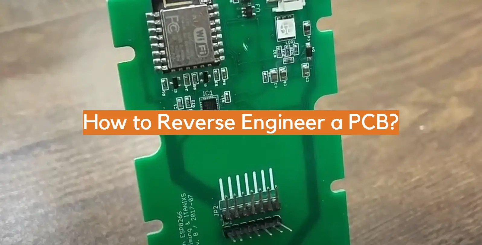
PCBs are often designed using specialized software, but sometimes it is necessary to reverse engineer an existing PCB design to understand its functionality or to create a replica. Reverse engineering a PCB can be a challenging task, and it requires a good understanding of electronics, PCB design, and the tools and techniques used in the process.
In this article, we will explore the process of reverse engineering a PCB in detail. We will discuss the tools and techniques used to create a schematic diagram from an existing PCB, how to identify and decode the components used on the board, and how to create a layout design for replicating the PCB.
We will also discuss the challenges and limitations of reverse engineering a PCB and provide some tips and best practices to help make the process more efficient and successful. Whether you are a hobbyist or a professional electronics engineer, this article will provide you with a solid foundation for understanding the process of reverse engineering a PCB and help you take on the challenge with confidence.
What Is PCB Reverse Engineering?
Reverse engineering typically involves using various tools and techniques to extract information from the PCB, such as circuit tracing, signal probing, and component identification. This information is then used to create a detailed schematic diagram and layout design that can be used to produce a new PCB that functions identically or similarly to the original.
PCB reverse engineering can be a complex and time-consuming process, especially for complex and densely packed PCBs. It requires a deep understanding of electronics, circuit design, and PCB manufacturing, as well as access to specialized equipment and software tools. However, it can also be a valuable tool for innovation, product improvement, and cost reduction, as it allows designers to build on existing designs and avoid reinventing the wheel.
Which Products Can Use PCB Reverse Engineering:
Instrumentation
These devices often require complex and precise electronics to function correctly, and PCB reverse engineering can be an invaluable tool for developing and improving them.
One common example of an instrument that can use PCB reverse engineering is a digital multimeter. A digital multimeter is a device that measures voltage, current, and resistance, and it uses a PCB to perform these measurements accurately. By reverse engineering the PCB, designers can identify the critical components and circuits that enable accurate measurements and improve or modify them to create more accurate or specialized versions of the device.
Another example of an instrument that can use PCB reverse engineering is a data acquisition system. A data acquisition system is a device that captures and stores data from sensors and other sources, and it often requires a custom PCB design to interface with different types of sensors and signal sources. By reverse engineering the PCB, designers can identify the critical components and circuits that enable data acquisition and improve or modify them to create more efficient or versatile versions of the device.
Communication
Communication devices are used to transmit and receive signals over various mediums, such as wired or wireless networks. These devices require complex and specialized electronics to function correctly, and PCB reverse engineering can be a valuable tool for developing and improving them.
One common example of a communication device that can use PCB reverse engineering is a modem. A modem is a device that converts digital data into analog signals for transmission over telephone lines or other communication channels. By reverse engineering the modem’s PCB, designers can identify the critical components and circuits that enable analog-to-digital conversion and improve or modify them to create faster or more reliable modems.
Another example of a communication device that can use PCB reverse engineering is a wireless router. A wireless router is a device that allows multiple devices to connect to a wireless network and access the internet. By reverse engineering the router’s PCB, designers can identify the critical components and circuits that enable wireless communication and improve or modify them to create more powerful or efficient routers.
Network Class
Network devices are used to manage and control communication networks, such as local area networks (LANs) or wide area networks (WANs). These devices require complex and specialized electronics to function correctly, and PCB reverse engineering can be a useful tool for developing and improving them.
By reverse engineering the switch’s PCB, designers can identify the critical components and circuits that enable network communication and improve or modify them to create faster or more reliable switches [2].
A router is a device that connects multiple LANs or WANs and allows them to communicate with each other. By reverse engineering the router’s PCB, designers can identify the critical components and circuits that enable network routing and improve or modify them to create more powerful or efficient routers.
Consumer Products
Consumer products are a broad category of devices that are used by individuals or households for various purposes, such as entertainment, communication, or automation. These devices often require custom and specialized electronics to function correctly, and PCB reverse engineering can be a valuable tool for developing and improving them.
A home automation system is a device that allows users to control various household devices, such as lights, thermostats, and security systems, from a central location. By reverse engineering the system’s PCB, designers can identify the critical components and circuits that enable home automation and improve or modify them to create more advanced or specialized systems.
By reverse engineering the console’s PCB, designers can identify the critical components and circuits that enable video game performance and improve or modify them to create faster or more powerful consoles.
Industrial Control
Industrial control devices are used to control and monitor various industrial processes, such as manufacturing, assembly, or testing. These devices require specialized and reliable electronics to function correctly, and PCB reverse engineering can be a valuable tool for developing and improving them.
A PLC (programmable logic controller) is a device that controls and monitors various industrial processes by using programmable logic and input/output modules. By reverse engineering the PLC’s PCB, designers can identify the critical components and circuits that enable industrial control and improve or modify them to create more advanced or specialized PLCs.
A motor controller is a device that controls the speed and direction of electric motors used in various industrial processes. By reverse engineering the motor controller’s PCB, designers can identify the critical components and circuits that enable motor control and improve or modify them to create more efficient or specialized motor controllers.
What Are the Benefits of Reverse Engineering PCB:
Helps PCB Design & Development
One of the most significant benefits of reverse engineering PCBs is that it helps improve the PCB design and development process. By taking an existing PCB and analyzing its structure, engineers can gain insights into how the board was designed, how it works, and how it could be improved. This information can be used to create a better version of the PCB or to develop a new, more advanced product.
Removal of Old Semiconductors
As technology evolves, older semiconductors become obsolete and are no longer manufactured. However, many older products still rely on these outdated components. Reverse engineering the PCB allows engineers to identify and replace these obsolete components with newer, more readily available ones. This not only improves the performance of the product but also extends its lifespan.
Save Time and Cost When Upgrading
Another benefit of reverse engineering PCBs is that it can save time and cost when upgrading an existing product. Rather than starting from scratch, engineers can analyze and replicate the existing PCB, making the necessary upgrades and improvements. This can save time and money compared to developing an entirely new PCB [3].
Enhance Your PCB Components
By reverse engineering a PCB, engineers can gain a better understanding of its components and how they work together. This knowledge can be used to optimize the performance of each component, leading to a more efficient and effective product. Additionally, engineers can identify any components that may be causing issues and replace them with better alternatives.
Develop a New Product Without Infringing on Another Company’s Intellectual Property Rights
Reverse engineering PCBs can also be a useful tool for developing new products without infringing on another company’s intellectual property rights. By analyzing an existing product’s PCB and reverse engineering it, engineers can create a new product that is similar but not identical to the original. This allows companies to avoid legal issues and still create a product that meets their customers’ needs.
Reconstruct and Preserve Outdated PCBs
Finally, reverse engineering PCBs can be used to reconstruct and preserve outdated PCBs. Many older products rely on unique, one-of-a-kind PCBs that are no longer manufactured. By reverse engineering these PCBs, engineers can recreate them and preserve the product’s functionality for years to come.
Why Reverse Engineer a PCB:
The PCB Operates Something Crucial
In many cases, the printed circuit board operates a crucial function in a product or system. If the PCB fails, the entire system can malfunction or stop working. When the original equipment manufacturer (OEM) no longer produces the PCB, it becomes necessary to reverse engineer it. Reverse engineering the PCB allows engineers and technicians to understand how the circuit works and identify potential failures, so they can create a replacement that operates as intended.
No Documentation/Data Exists
In some cases, the original documentation or data for a PCB may be lost or not available. Without proper documentation, it can be difficult to troubleshoot or repair the circuit. Reverse engineering the PCB can provide a detailed understanding of how the circuit functions and can help create documentation for future reference. This documentation can also be useful for future design and engineering projects.
No Professional Knows What to Do With It
Occasionally, a PCB may be too complex or unique, and no professional knows how to handle it. In such cases, reverse engineering the PCB can be a useful tool for understanding its functions and components. Once reverse-engineered, engineers and technicians can understand how the circuit functions and can make modifications or replacements as needed.
PCB Redesign
Another reason to reverse engineer a PCB is to redesign it for better performance or efficiency. By analyzing the components and connections of an existing PCB, engineers can identify weaknesses or areas of inefficiency. They can then redesign the PCB to improve its performance, extend its lifespan, or reduce manufacturing costs [4].
Obsolete Components
As technology evolves, older components become obsolete and are no longer manufactured. This can be a problem when trying to repair or replace older PCBs that rely on these components. Reverse engineering the PCB can help identify these obsolete components and provide information on suitable replacement components. This can extend the life of older equipment or reduce the cost of manufacturing replacement PCBs.
Intellectual Property Protection
Reverse engineering PCBs can also help protect intellectual property. By reverse engineering a PCB, engineers can understand how it works and identify potential issues or weak points. They can then make modifications to the PCB to improve its performance or efficiency without infringing on the original manufacturer’s intellectual property rights.
How to Reverse Engineer a PCB:
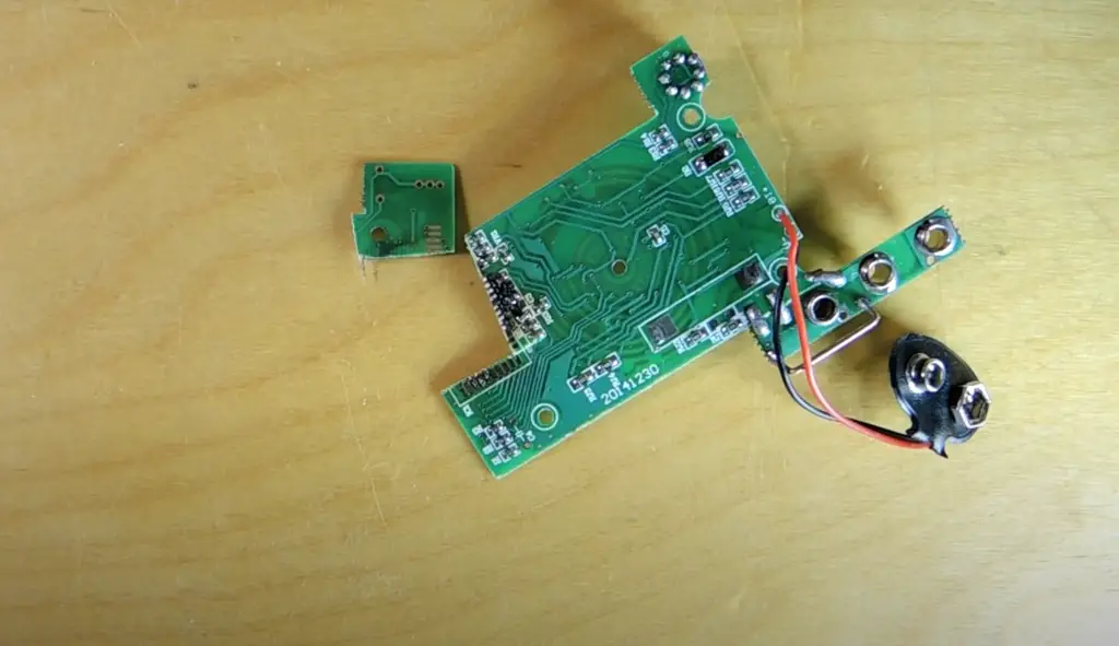
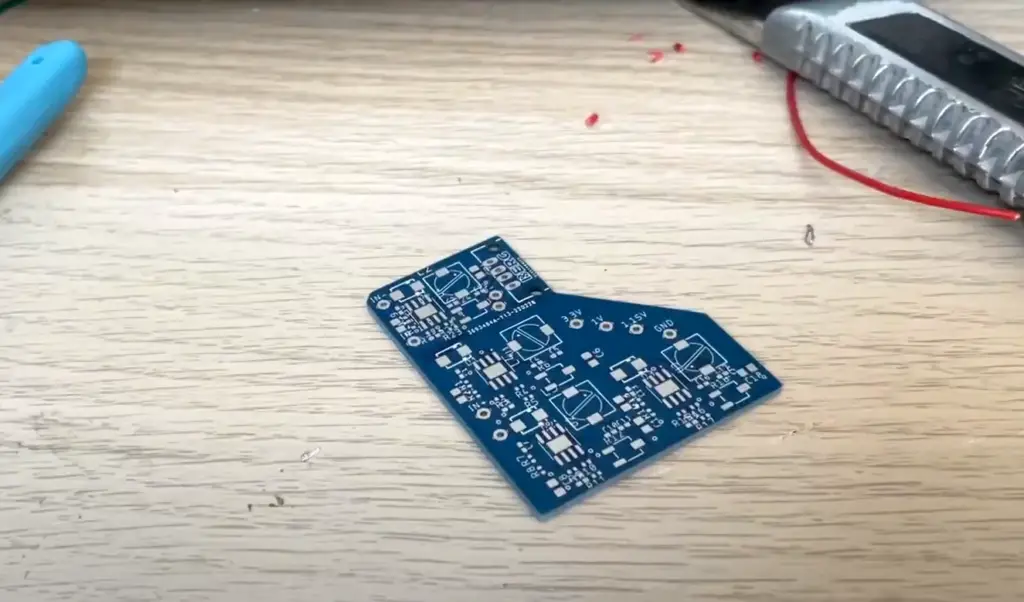
Step 1: Draw, Scan, or Photograph the PCB for Image Prep
The first step in reverse engineering a PCB is to obtain a clear and accurate image of the PCB layout. This can be done by either drawing the PCB manually or by using a scanner or camera to capture an image of the PCB. In some cases, the manufacturer may provide a schematic diagram or a datasheet for the PCB, which can also be used as a reference.
It is important to ensure that the image captured is of high quality, with clear visibility of all the components and their connections. Any blurred or missing details can make it difficult to reverse engineer the PCB accurately.
Step 2: Upload the Image
Once the image of the PCB is obtained, it needs to be uploaded to a PCB software program, which can be used to create the layout and schematic of the PCB. There are several PCB software programs available in the market, such as Eagle PCB, Altium Designer, and KiCAD.
Step 3: Construct the Layout
The next step in reverse engineering a PCB is to construct the layout of the PCB using the software program. The software program will have a set of tools and features that can be used to create the layout of the PCB accurately.
It is important to ensure that the layout is constructed to the exact dimensions of the original PCB, including the size and shape of the board and the placement of the components. Any discrepancies in the layout can affect the functionality of the PCB.
Step 4: Create Schematics
The final step in reverse engineering a PCB is to create the schematics of the PCB. The schematics provide a visual representation of the connections between the various components on the PCB.
To create the schematics, the software program will provide a set of symbols and libraries that can be used to represent the different components on the PCB. It is important to ensure that the symbols used are accurate and represent the exact components used on the original PCB.
Once the schematics are created, they can be cross-checked with the original PCB to ensure accuracy. Any discrepancies should be corrected to ensure that the replica PCB functions as intended.
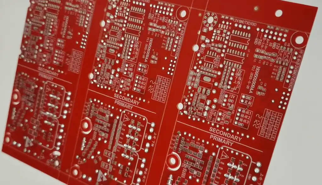
Multilayer PCB Reverse Engineering Operation Method:
Step 1: Preparation
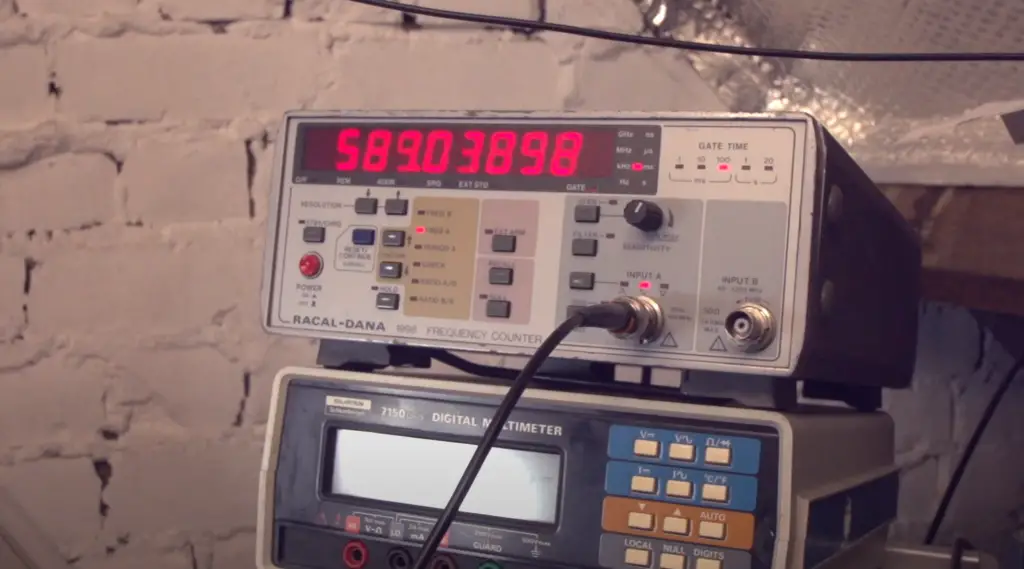
Before starting the reverse engineering process, engineers need to prepare the necessary equipment and software. The equipment needed includes a microscope, a hot air gun, tweezers, and a multimeter. The software needed includes a copy board software and schematic capture software.
Once the equipment and software are ready, the engineer needs to select the appropriate PCB to reverse engineer. The selected PCB should be of the same type and model as the original PCB to be reverse-engineered. If possible, engineers should also gather as much information about the original PCB as possible, such as its schematic and layout.
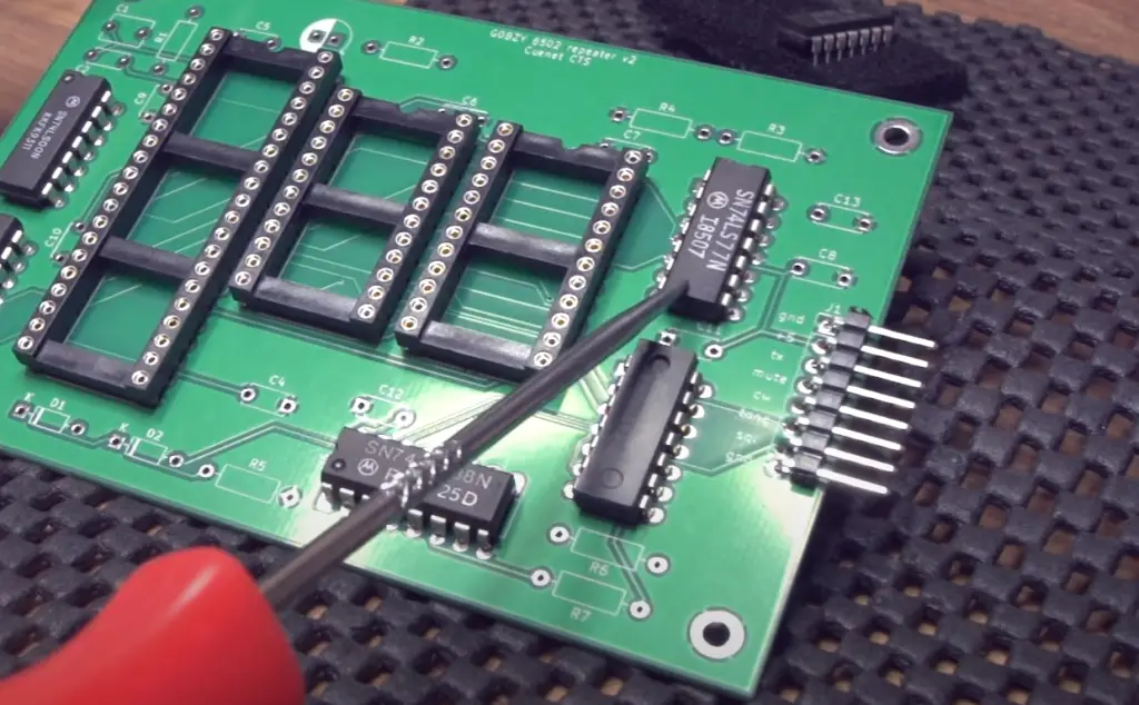
Step 2: Disassemble components and make BOM
The next step is to disassemble the components on the PCB and create a Bill of Materials (BOM). Engineers need to use a microscope and a hot air gun to remove the components from the PCB carefully. They should also take note of the orientation and position of each component and label them accordingly. Once all the components are removed, engineers can create a BOM that lists all the components used on the PCB.
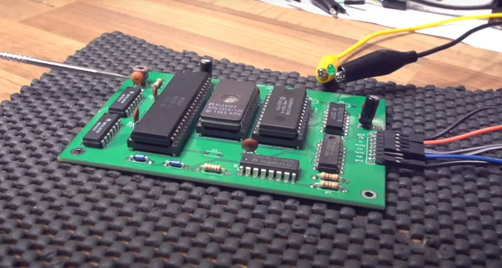
Step 3: Removing tin on the surface
After disassembling the components and creating a BOM, engineers need to remove the tin on the surface of the PCB. This is done to expose the traces and vias on the PCB, making it easier to trace the connections. Engineers can use a hot air gun or a soldering iron to remove the tin. They should be careful not to overheat the PCB and damage the traces and vias [6].
Step 4: Real-time operation in the copy board software
The next step is to use copy board software to trace the connections on the PCB. The copy board software enables engineers to create a digital copy of the PCB layout and schematic. To do this, engineers need to connect the PCB to a power supply and a multimeter to measure the voltage and current on the traces.
Engineers can then use the copy board software to trace the connections on the PCB in real time. They should start by identifying the power and ground planes and then trace the connections from there. The copy board software will generate a digital copy of the PCB layout and schematic as engineers trace the connections.
Step 5: Check
The final step is to check the accuracy of the digital copy of the PCB layout and schematic. Engineers should compare the digital copy with the original PCB layout and schematic to ensure that there are no errors or omissions. They should also check the BOM to ensure that all the components are accounted for.
Once engineers are satisfied with the accuracy of the digital copy, they can use it to create a new PCB layout and schematic. They can also use the BOM to source the components needed to recreate the PCB.
Why Would Any Engineer Want to Engage in Reverse Engineering PCB:
There Is No Sufficient Data
One of the most common reasons engineers might engage in PCB reverse engineering is a lack of sufficient data. Engineers may not always have access to the design files, schematics, or documentation of a PCB they need to work with.
For example, if an engineer is working with an outdated or obsolete product, they may not have access to the original design files or documentation. In these cases, the engineer may need to reverse engineer the PCB to understand how it works and what components are used.
Another scenario where engineers might need to engage in PCB reverse engineering is when they are working with a product that was not designed by their company.
For instance, an engineer may be asked to troubleshoot or repair a PCB for a customer, but they may not have access to the design files or documentation for that product. In this case, the engineer may need to reverse engineer the PCB to understand its design and functionality.
If No Professional Can Handle the PCB
Another reason why an engineer might want to engage in PCB reverse engineering is if no professional can handle the PCB. In some cases, a PCB may be too complex or specialized for a professional to handle.
For example, if a PCB is used in a military or aerospace application, it may be too complex for most professionals to understand or work with. In these cases, an engineer may need to engage in PCB reverse engineering to understand how the PCB works and what components are used.
Another scenario where an engineer may need to engage in PCB reverse engineering is if the PCB is damaged or degraded. In some cases, a damaged or degraded PCB may be too complex or specialized for most professionals to repair or replace. In these cases, an engineer may need to engage in PCB reverse engineering to understand the PCB’s design and functionality and develop a solution for repairing or replacing the PCB.
For a Very Important Reason
Finally, an engineer may want to engage in PCB reverse engineering for a very important reason. For example, an engineer may want to improve or modify a product to make it safer, more reliable, or more efficient. The engineer may need to engage in PCB reverse engineering to identify the critical components and circuits that enable product functionality and improve or modify them to create a better product.
Another scenario where an engineer may want to engage in PCB reverse engineering is if they suspect a PCB is being used for malicious purposes. For instance, if an engineer suspects that a PCB is being used to steal or manipulate data, they may want to engage in PCB reverse engineering to identify any malicious components or circuits and develop a solution for preventing or mitigating their effects.
FAQ
1. Is it possible to reverse engineer a PCB?
Yes, it is possible to reverse engineer a PCB. The process involves analyzing an existing PCB to determine its functionality, identifying and decoding the components used on the board, and creating a schematic diagram and layout design for replicating the PCB [7].
2. How do you reverse engineer an electronic device?
To reverse engineer an electronic device, you need to analyze its physical structure, electrical signals, and software code. This involves disassembling the device, identifying and decoding the components, tracing the electrical signals, and analyzing the firmware or software code. Reverse engineering tools and techniques such as oscilloscopes, logic analyzers, and disassemblers are commonly used in the process.
3. Is copying PCB illegal?
It depends on the context. Copying a PCB without permission from the original designer or copyright holder may be considered copyright infringement and could be illegal. However, if the PCB is no longer protected by copyright or if the copying is for personal or educational purposes, it may be legal.
4. Can reverse engineering be forbidden?
Reverse engineering is generally legal, and in some cases, it is protected under fair use or other exemptions. Nevertheless, there are some instances where reverse engineering is forbidden, such as when it violates patent or trade secret laws or when it is used for illegal activities.
5. How do you reverse engineer yourself?
Reverse engineering oneself is a process of introspection and self-analysis to understand one’s thought processes, behaviors, and habits. This can involve journaling, self-reflection exercises, therapy, or other forms of self-improvement practices.
6. Is reverse engineering just copying?
Reverse engineering is more than just copying. It involves analyzing an existing product or system to understand its functionality, identifying and decoding the components used, and creating a new design that replicates the original functionality or improves upon it.
7. Is reverse engineering legal but unethical?
Reverse engineering can be both legal and ethical or illegal and unethical, depending on the circumstances. If reverse engineering is done for legitimate purposes such as research or interoperability, it is generally considered legal and ethical. But, if it is done to steal intellectual property or to create counterfeit products, it is illegal and unethical [8].
8. Is it easy to reverse engineer?
Reverse engineering can be a challenging and time-consuming process, requiring a deep understanding of the product or system being analyzed, as well as specialized tools and techniques. Nevertheless, with the right skills and resources, it is possible to successfully reverse engineer a product or system.
9. What malware is difficult to reverse engineer?
Malware that employs advanced obfuscation or anti-analysis techniques, such as packers, encryption, or virtualization, can be difficult to reverse engineer. Additionally, malware that uses rootkits or other stealth techniques to hide its presence on a system can also be challenging to detect and analyze.
10. Can you repurpose a PCB?
Yes, it is possible to repurpose a PCB for a different application or function. This involves analyzing the PCB’s existing design, identifying the necessary modifications, and making the necessary changes to the layout and components. Repurposing a PCB can be a cost-effective way to develop new products or prototypes.
11. Can a PCB function without a solder mask?
Yes, a PCB can function without a solder mask, but it is not recommended.
Without a solder mask, the copper traces are exposed, making them more vulnerable to damage during handling and assembly. Additionally, the solder mask provides a visual contrast that makes it easier to inspect and troubleshoot the PCB [9].
12. Is PCB reverse engineering legal?
The legality of PCB reverse engineering depends on the context. In some cases, reverse engineering a PCB may be protected under fair use or other exemptions, especially if it is done for research, education, or interoperability purposes. But if reverse engineering is done to infringe on someone’s intellectual property rights or to create counterfeit products, it may be illegal and subject to legal action.
13. Do PCBs expire?
PCBs do not have a specific expiration date, but their lifespan can be affected by various factors such as environmental conditions, mechanical stress, and exposure to corrosive materials. PCBs can also become obsolete as technology advances, making them less useful for newer applications. If properly stored and maintained, PCBs can last for many years [10].
14. Can a 3D scanner help with reverse engineering?
Yes, a 3D scanner can be a useful tool for reverse engineering, especially for analyzing the physical structure and dimensions of a PCB or other object. A 3D scanner can generate a detailed 3D model of the object, which can be imported into CAD software for further analysis and modification.
Additionally, a 3D scanner can help identify the location and orientation of components on the PCB, which can be useful for creating a layout design.
However, 3D scanning alone may not be sufficient for reverse engineering a complex electronic system, as it does not provide information about the electrical signals or software code [11].
Useful Video: How I Reverse-Engineer Simple PCB Boards
References
- https://www.raypcb.com/pcb-reverse-engineering/
- https://www.ourpcb.com/reverse-engineering-pcb.html
- https://www.reddit.com/r/PrintedCircuitBoard/comments/edhtgm/how_i_reverse_engineer_pcbs/
- https://www.mclpcb.com/blog/how-to-reverse-engineer-a-pcb/
- https://www.electronicdesign.com/markets/automation/article/21249478/mermar-electronics-reverse-engineering-a-printed-circuit-board
- https://www.instructables.com/How-to-reverse-engineer-a-schematic-from-a-circuit/
- https://en.wikipedia.org/wiki/PCB_reverse_engineering
- https://www.chinapcbcopy.com/pcb-reverse-engineering/
- https://www.candorind.com/how-to-reverse-engineer-a-pcb/
- https://scancad.net/pcb-reverse-engineering/
- https://www.pcbtok.com/pcb-reverse-engineering/