In the world of printed circuit board (PCB) design and manufacturing, there are several types of packaging options available for electronic components. One of the most popular types is Ball Grid Array (BGA), which has gained widespread use due to its numerous advantages over other packaging options. A BGA package consists of an array of small metal balls, or solder balls, that are arranged in a grid pattern on the bottom of the component. These balls serve as the electrical and mechanical connections between the component and the PCB.
BGA technology offers several benefits over traditional through-hole or surface-mount technology. First and foremost, BGAs have a much higher pin density, meaning that they can accommodate more connections in a smaller area. This makes them ideal for use in high-performance electronic devices, such as smartphones and gaming consoles, where space is at a premium. Additionally, BGAs offer superior thermal and electrical performance, as the solder balls provide a more direct path for heat dissipation and signal transmission.
In this article, we will explore the intricacies of BGA technology, including its history, advantages and disadvantages, and best practices for designing and manufacturing BGA-based PCBs.
What is Ball Grid Array or BGA?
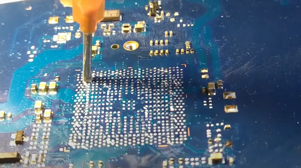
This type of packaging eliminates the need for holes in the PCB, allowing it to be smaller and more compact. Additionally, BGA packages have a higher pin count than other packages, making them ideal for applications requiring many connections between components. As with any technology, there are pros and cons associated with using BGA packages [1].
Pros:
- Due to their high pin count, BGA packages allow for increased functionality in a small area;
- They provide improved signal integrity by reducing crosstalk between components;
- BGA packages have a high component density, allowing for more components to be placed in a given area;
- They are cost-effective and easy to assemble;
- BGA packages are highly reliable and durable;
Cons:
- BGA packages require special tools for assembly, making it difficult to make changes once the PCB is assembled;
- The reflow process used for BGA packaging requires precise temperature control, which can lead to errors if not done properly;
- Due to its small size, repairing or replacing a component on a board using BGA packages can be challenging;
- Debugging circuits with BGA packages can be difficult due to their compact size;
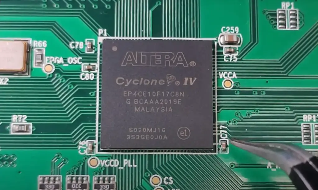
Ball Grid Array (BGA) Soldering
Ball Grid Array or BGA is a type of surface-mount packaging used for integrated circuits. It is a form of printed circuit board that uses an array of metal pads on one side and small metallic balls to connect them to the components on the other side.
BGA soldering is required when attaching these tiny components to the boards, and it requires special equipment and skill. The process involves placing the component with its connecting pins against the copper pads, which are then heated with a hot air gun until they melt together. This forms a strong connection that can last up to 20 years in certain conditions [2].
The most important part of this process is making sure that all the connections are properly aligned since any misalignment can cause poor connections, which can lead to the device performance issues and even damage to the IC.
BGA soldering is a delicate process and requires patience and precision in order for it to be done correctly. It can take some time for the solder paste to properly heat and cool, but once it is complete, your device should work as expected.
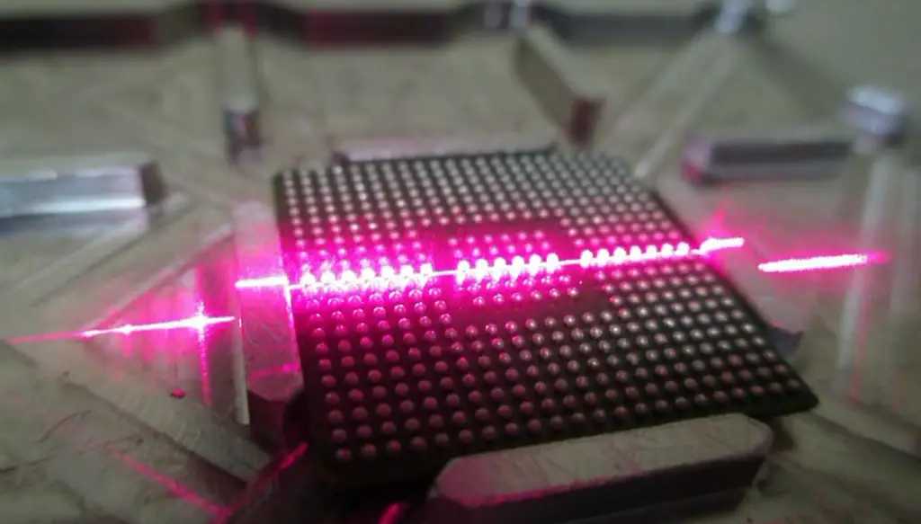
Reasons For BGA Being Popular
This surface-mount technology is widely used in electronic circuits, as it has several advantages over traditional through-hole mounting methods.
The most obvious benefit of BGA is its space efficiency. Compared to through-hole packages, BGA is much smaller and takes up less board area, allowing for faster routing and assembly processes. In addition, due to their small size and lack of external leads, BGAs are also much more resistant to physical damage caused by dust and handling during installation. Finally, since there are no external leads sticking out from the back side of the chip package, BGAs are much easier to protect from environmental contaminants such as humidity and moisture.
BGA also offers improved electrical performance due to its higher connection density. The connections between the chip and board are made through small solder balls, which can be placed closer together than traditional leads, reducing signal crosstalk. In addition, BGA packages generally have more layers on their inner structures than through-hole designs, allowing for better resistance to electromigration and providing superior thermal transfer characteristics [3].
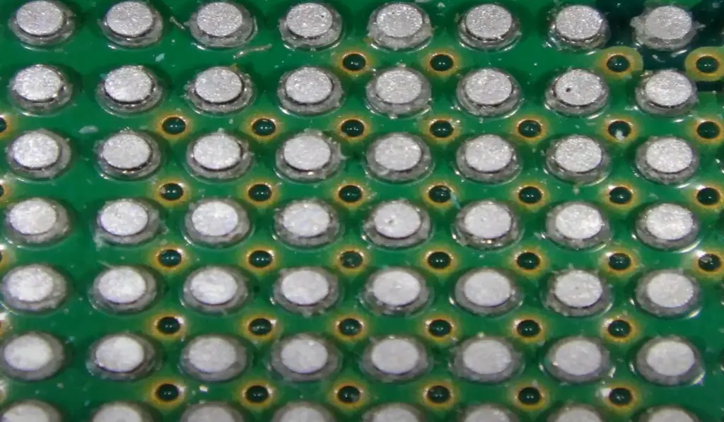
Ball Grid Array (BGA) Features:
Less Thermal Resistance
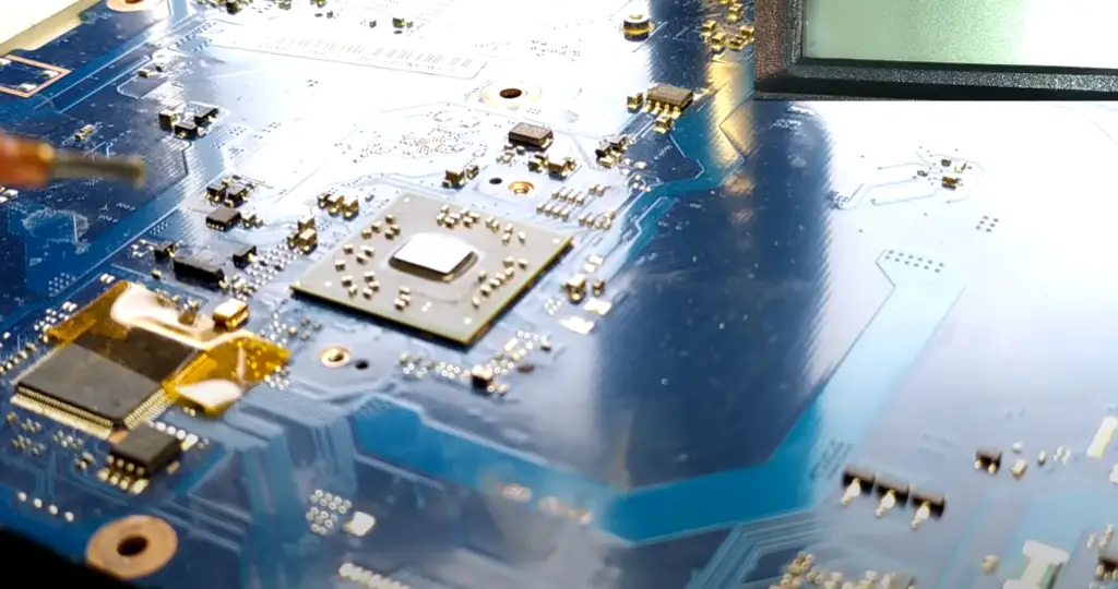
One of the primary advantages of BGA technology is its ability to dissipate heat more efficiently than other packaging options. This is due to the direct connection between the component and the PCB through the solder balls. Unlike through-hole or surface-mount components, which rely on pins or pads to transfer heat to the PCB, BGA components have a much shorter thermal path, which results in less thermal resistance.
In traditional through-hole or surface-mount components, the heat generated by the component must first travel through the pin or pad, then through the PCB trace, before finally dissipating into the surrounding environment. This can lead to a significant amount of thermal resistance, which can cause the component to overheat and fail. With BGA technology, however, the heat generated by the component is transferred directly to the PCB through the solder balls, resulting in less thermal resistance and improved heat dissipation.
Less thermal resistance is particularly important in high-performance electronic devices, such as gaming consoles and smartphones, which generate a significant amount of heat during operation. By using BGA components, designers and manufacturers can ensure that their devices can operate at high temperatures without the risk of failure due to overheating.
Better Performance at High Speeds
Another advantage of BGA technology is its ability to provide better performance at high speeds. This is due to the shorter electrical path between the component and the PCB through the solder balls. In traditional through-hole or surface-mount components, the electrical path between the component and the PCB can be relatively long, which can lead to signal degradation and other performance issues at high frequencies.
With BGA technology, however, the electrical path between the component and the PCB is much shorter, which results in improved signal integrity and better performance at high speeds. This is particularly important in high-speed communication applications, such as Ethernet and USB, where signal integrity is critical to maintaining reliable data transfer.
In addition to providing better performance at high speeds, BGA technology also allows for higher pin densities, which can accommodate more connections in a smaller area. This is particularly useful in applications where space is at a premium, such as mobile devices and wearables.
Higher Reliability
Finally, BGA technology offers higher reliability than other packaging options. This is due to the direct connection between the component and the PCB through the solder balls, which provides a more secure mechanical connection than through-hole or surface-mount components.
In traditional through-hole or surface-mount components, the pins or pads can become loose or damaged over time, leading to intermittent connections or complete failures. With BGA technology, however, the solder balls provide a more secure mechanical connection, which is less prone to failure due to mechanical stress or vibration.
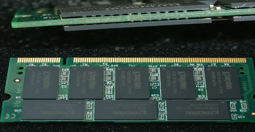
In addition to providing a more secure mechanical connection, BGA technology also allows for better inspection and testing of the solder joints. This is because the solder balls are visible from the top of the component, allowing for visual inspection and testing of the connections [4].
Types of BGA:
1) PBGA (Plastic Ball Grid Array)
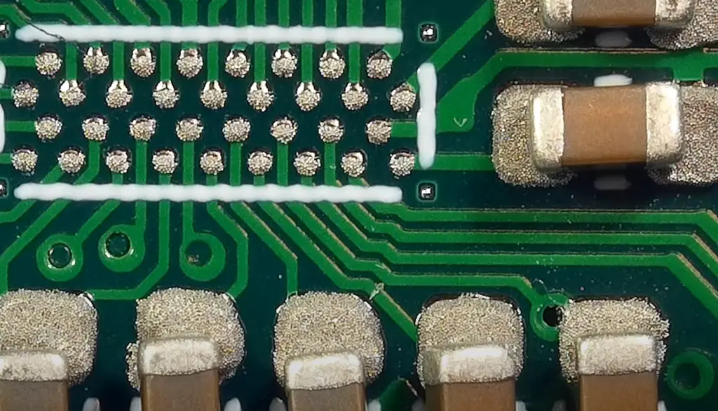
PBGA or Plastic Ball Grid Array is a type of BGA package that uses a plastic substrate material for the component’s packaging. This material is less expensive than ceramic and is preferred for low-cost applications. PBGA components have a large number of solder balls, which allows for more connections between the component and the PCB, improving the overall performance of the device. They are also known for their good thermal performance and can be used in a wide range of applications, such as consumer electronics, telecommunications, and automotive electronics.
2) CBGA (Ceramic Ball Grid Array)
CBGA or Ceramic Ball Grid Array is a BGA package that uses a ceramic substrate material for the component’s packaging. Ceramics is an excellent material for high-performance applications as it has good thermal conductivity and can withstand high temperatures. CBGA components are preferred for military, aerospace, and medical applications due to their reliability and durability. They also have a long lifespan and can function under harsh conditions, making them suitable for applications that require high reliability.
3) TBGA (Tape Ball Grid Array)
TBGA or Tape Ball Grid Array is a type of BGA package that uses a tape-based packaging technology. It is a low-cost solution and is commonly used in mobile devices, such as smartphones and tablets. The tape-based package provides a high level of flexibility, which is required in applications where space is limited. TBGA components have a smaller footprint than other types of BGA packages and can be mounted on both sides of the PCB, further increasing the board’s density.
4) EBGA (Enhanced Ball Grid Array)
EBGA or Enhanced Ball Grid Array is a type of BGA package that uses a combination of ceramic and organic materials for the component’s packaging. The ceramic layer provides good thermal conductivity, while the organic layer allows for more flexibility and better electrical performance. EBGA components are commonly used in high-performance applications that require a combination of reliability and flexibility, such as server systems, networking equipment, and high-end gaming systems [5].
5) FC-BGA (Flip Chip Ball Grid Array)
FC-BGA or Flip Chip Ball Grid Array is a type of BGA package that uses flip-chip technology to mount the component on the PCB. In this package, the component is flipped and mounted directly onto the PCB using solder bumps instead of solder balls. This technology provides better electrical performance and can handle higher frequencies than other types of BGA packages. FC-BGA components are commonly used in high-speed applications, such as graphics processing units (GPUs), digital signal processors (DSPs), and field-programmable gate arrays (FPGAs).
6) MBGA (Metal Ball Grid Array)
MBGA or Metal Ball Grid Array is a type of BGA package that uses metal solder balls instead of conventional tin-lead balls. This type of BGA package has a higher melting point than conventional BGA packages, making it suitable for applications that require high-temperature processing. MBGA components are commonly used in automotive and industrial applications, where high-temperature environments are common.
7) Micro BGA
Micro BGA is a type of ball grid array that is much smaller in size than the other types. It is also known as uBGA or μBGA. The pitch of a micro BGA is usually between 0.5mm and 1.0mm, which makes it ideal for small devices such as mobile phones, digital cameras, and handheld gaming consoles.
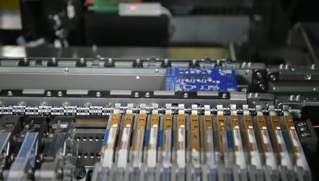
The process of manufacturing a micro BGA is similar to that of a standard BGA. However, due to its small size, the components are much harder to place accurately, and the soldering process can be more difficult. To overcome these challenges, specialized equipment is used to ensure accurate placement and proper soldering.
FAQ
1. How is the BGA package made?
The process of making a BGA package involves several steps, including semiconductor fabrication, substrate manufacturing, and assembly.
The first step in the process is the fabrication of the semiconductor die, which is typically made using a combination of photolithography and etching techniques. Once the die is fabricated, it is mounted onto a small substrate made of ceramic or other materials.
The substrate is then coated with a layer of solder mask, leaving only the areas where the solder balls will be attached exposed. A stencil is then used to apply a paste of solder balls onto the exposed areas of the substrate.
The next step in the process is the reflow soldering of the BGA component onto the printed circuit board (PCB). This is typically done using a specialized tool called a BGA rework station, which uses a combination of heat, pressure, and precision alignment to ensure that the solder balls adhere to the copper pads on the PCB.
2. What is the difference between BGA and FBGA?
The main difference between BGA (ball grid array) and FBGA (fine-pitch ball grid array) is the spacing between the solder balls on the substrate. FBGA components have a tighter pitch, meaning that the distance between each ball is smaller, typically between 0.5mm and 0.8mm. This allows for a higher pin density and better electrical performance, making FBGA components ideal for high-speed communication applications [6].
3. What are the BGA package sizes?
The size of the package is typically measured in millimeters and can vary depending on the application and the specific component being used.
Some common BGA package sizes include:
- 2mm x 2mm: This is a very small BGA package that is often used for small, low-power components such as microcontrollers and sensors;
- 10mm x 10mm: This is a larger BGA package that is often used for high-performance components such as microprocessors and memory chips;
- 27mm x 27mm: This is a very large BGA package that is often used for components such as graphics processing units and other high-performance communication devices [7];
4. What is a pin grid array vs a ball grid array?
Pin grid array (PGA) and ball grid array (BGA) are two different types of packaging technologies used for electronic components.
In a PGA, the component is mounted onto a substrate with a grid of metal pins on the bottom of the component. The pins are inserted into holes on the printed circuit board (PCB) and soldered in place to form a mechanical and electrical connection.
In contrast, a BGA uses a grid of small spherical balls made of solder to connect the component to the PCB. The balls are located on the bottom of the component and are melted during a reflow soldering process to create a strong mechanical and electrical connection.
BGA components have become increasingly popular in recent years due to their higher pin density, better thermal management, and improved electrical performance compared to PGA components.
5. What is PGA vs LGA?
PGA (pin grid array) and LGA (land grid array) are two different types of packaging technologies used for electronic components.
In a PGA, the component is mounted onto a substrate with a grid of metal pins on the bottom of the component. The pins are inserted into holes on the printed circuit board (PCB) and soldered in place to form a mechanical and electrical connection.
On the contrary, an LGA uses a grid of small metal pads on the bottom of the component to connect to the PCB. The pads are located on the surface of the component and are pressed against matching pads on the PCB to form a mechanical and electrical connection.
LGA components have become increasingly popular in recent years due to their higher pin density, better thermal management, and improved electrical performance compared to PGA components.
6. What is a BGA socket?
A BGA socket is a specialized component that allows for the easy insertion and removal of a ball grid array (BGA) component from a printed circuit board (PCB).
The socket consists of a plastic or ceramic housing with a grid of small spring-loaded pins that align with the solder balls on the bottom of the BGA component. When the component is inserted into the socket, the spring-loaded pins compress and make contact with the solder balls, creating a secure mechanical and electrical connection.
BGA sockets are commonly used for prototyping and testing BGA components, as they allow for easy replacement of the component without the need for soldering or other complex assembly techniques.
7. What is the full form of BGA in PCB?
BGA components are used in a wide range of high-performance applications where reliability, signal integrity, and thermal management are critical.
8. Is BGA free?
No, BGA (ball grid array) components are not free. Like all electronic components, they have a cost associated with their design, manufacture, and distribution.
The cost of a BGA component can vary depending on a number of factors, including the complexity of the component, the size of the package, the quantity purchased, and the manufacturer’s pricing strategy.
9. What is the smallest BGA package?
The smallest BGA package currently available is the 0.4mm pitch BGA. This package has a ball pitch (the distance between the centers of two adjacent solder balls) of just 0.4mm, making it ideal for use in small, space-constrained applications.
10. What is the minimum BGA pad size?
The minimum BGA pad size is determined by the pitch of the component. The pitch is the distance between the centers of two adjacent solder balls, and the pad size must be at least equal to or larger than the pitch to ensure reliable electrical and mechanical connections.
For example, a BGA with a 0.5mm pitch would require a minimum pad size of 0.5mm x 0.5mm.
11. What is an example of BGA?
An example of a BGA component is the Intel Core i7 processor. This processor features a BGA package with over a thousand solder balls, which provide the electrical and mechanical connections between the processor and the PCB.
BGA components are used in a wide range of high-performance applications, including microprocessors, memory chips, graphics processing units, and other communication devices.
12. Can BGA be replaced?
Yes, BGA components can be replaced, but the process is more complex than replacing a through-hole or surface-mount component. BGA components are typically soldered to the PCB using a reflow soldering process, which melts the solder balls and creates a strong mechanical and electrical connection.
To replace a BGA component, the old component must be removed using specialized equipment, such as a rework station or hot air gun. The new component is then placed on the PCB and soldered in place using the same reflow soldering process.
13. Do you need to paste for BGA?
Yes, solder paste is required for attaching a BGA component to a printed circuit board (PCB). The solder paste is applied to the pads on the PCB using a stencil, and the BGA component is then placed onto the pads. During the reflow soldering process, the solder paste melts and creates a strong mechanical and electrical connection between the component and the PCB.
14. What is the difference between QFP and BGA packages?
QFP (quad flat package) and BGA (ball grid array) are two different types of packaging technologies used for electronic components.
In a QFP package, the component has leads on all four sides of the package that are bent outwards and inserted into holes on the printed circuit board (PCB). The leads are then soldered in place to form a mechanical and electrical connection.
A BGA uses a grid of small spherical balls made of solder to connect the component to the PCB. The balls are located on the bottom of the component and are melted during a reflow soldering process to create a strong mechanical and electrical connection.
The main difference between QFP and BGA packages is the number of pins and the pitch of the package. BGA packages typically have a higher pin density and a smaller pitch than QFP packages, making them ideal for high-performance applications.
15. How do you solder a ball grid array?
Soldering a ball grid array (BGA) component to a printed circuit board (PCB) requires a specialized reflow soldering process.
Here are the steps involved:
- Apply solder paste to the pads;
- Place the BGA component on the pads, ensuring that it is aligned correctly;
- Heat the PCB and the BGA component in a reflow oven or a rework station. The temperature and time required for the reflow process will depend on the type of solder paste and the size of the BGA component;
- The solder paste will melt, and the solder balls on the BGA component will form a mechanical and electrical connection with the pads on the PCB;
- Once the solder has solidified, inspect the connections to ensure that there are no solder bridges or cold joints;
Soldering a BGA component requires specialized equipment and expertise, and should only be attempted by experienced technicians.
16. What is the difference between BGA and CSP?
In a BGA package, the component has a grid of small spherical balls made of solder that connects the component to the printed circuit board (PCB). The balls are located on the bottom of the component and are melted during a reflow soldering process to create a strong mechanical and electrical connection.
A CSP is a type of package where the component is roughly the same size as the die that it contains. CSP packages typically have a smaller footprint and a thinner profile than BGA packages.
The main difference between BGA and CSP packages is the size and shape of the package. BGA packages are typically larger and have a higher pin density than CSP packages, while CSP packages are smaller and more compact.
17. What is the biggest limitation of array data structure?
The biggest limitation of an array data structure is its fixed size. Once an array is created, its size cannot be changed dynamically. This means that if the array is too small to hold all of the data that needs to be stored, a new, larger array must be created and the data must be copied over. This can be inefficient and time-consuming, particularly if the array is large.
Another limitation of an array is that it can only hold data of a single data type. For example, an array of integers cannot hold a mixture of integers and strings.
Finally, accessing elements in an array can be slow if the array is large and the data is scattered throughout the array. This is because arrays are stored in contiguous memory locations, and accessing an element in the middle of the array requires traversing all of the elements that come before it.
18. How many times can a BGA be reworked?
The number of times that a BGA component can be reworked depends on a number of factors, including the quality of the component, the skill of the technician, and the type of rework equipment used.
In general, BGA components can be reworked multiple times as long as they are not damaged during the removal and reinstallation process. However, each time a BGA component is reworked, there is a risk of damaging the solder balls or the component itself, which can reduce the reliability of the component.
19. How do you reduce BGA voids?
BGA voids are small air pockets that can form between the solder balls and the PCB during the reflow soldering process. Voids can reduce the mechanical and electrical reliability of the BGA component, so it is important to minimize their occurrence.
Here are some tips for reducing BGA voids:
- Use a high-quality solder paste that is designed to reduce voiding;
- Optimize the reflow profile to ensure that the solder paste melts and flows correctly;
- Use a vacuum-assisted reflow process to remove air from the solder paste;
- Ensure that the PCB and the BGA component are properly cleaned and free of contaminants;
- Use a proper stencil design to ensure that the correct amount of solder paste is applied to each pad;
- Consider using a reflow oven with a nitrogen atmosphere to reduce the amount of oxygen in the environment;
20. Why is BGA used in PCB?
BGA is used in PCB (printed circuit board) packaging for several reasons. One of the main benefits of BGA is its high pin density, which allows for more connections between the component and the PCB. This can lead to improved performance and functionality in electronic devices.
BGA packages also have a lower profile than other types of packages, which can be important in space-constrained applications. BGA packages can also handle higher frequencies and speeds than other types of packages, making them well-suited for high-performance applications.
Finally, BGA packages offer better thermal performance than other types of packages. The solder balls on the bottom of the component provide a more direct path for heat to dissipate from the component to the PCB, which can improve the overall reliability of the device.
21. Can a BGA processor be replaced?
A BGA (ball grid array) processor can be replaced, but it requires specialized equipment and expertise. In order to replace a BGA processor, the existing component must be removed from the PCB and a new component must be installed in its place.
Removing a BGA component requires the use of a rework station or other specialized equipment to heat the component and melt the solder balls that connect it to the PCB. The component must then be carefully removed without damaging the PCB or any other components on the board.
Installing a new BGA component also requires specialized equipment and expertise, as the component must be aligned correctly and reflowed onto the PCB using a soldering process. It is important to ensure that the new component is compatible with the existing PCB and that the reflow process is optimized to minimize the risk of voids or other defects.
22. What is the best way to explain an array?
The values in an array are stored in contiguous memory locations, which allows them to be accessed using a single variable name and an index value that specifies the position of the value in the array.
Arrays can be used to store and manipulate large amounts of data efficiently. They are often used in programming languages to represent lists, tables, and other structured data. Arrays can also be used to implement other data structures, such as stacks, queues, and linked lists.
Useful Video: What is BGA package? | PCB Knowledge
References
- https://en.wikipedia.org/wiki/Ball_grid_array
- https://blog.matric.com/ball-grid-array-pcb-packaging
- https://www.raypcb.com/different-types-of-bga-ball-grid-array-packages/
- https://madpcb.com/glossary/bga-ball-grid-array/
- https://www.fs-pcba.com/plastic-ball-grid-array/
- https://www.electronicsandyou.com/blog/ball-grid-array-bga-package.html
- https://www.analog.com/en/app-notes/ball-grid-array-bga-packages-and-pcb-design-guidelines.html










Leave a Reply