Inverters are a critical part of many electronic circuits. There are many different types of inverters, but one of the most common is the CMOS inverter. In this article, we will discuss what a CMOS inverter is, and we will provide some tips on how to design circuits with them.
CMOS Inverter Definition
In terms of applications, CMOS inverters are used for many purposes in digital electronic systems such as controlling power supplies, working with memory cells, and decoding signals from other devices. They can also be used as switches in circuits, to create logic gates, and to make digital clocks. [1], [2]
How CMOS Inverters Work
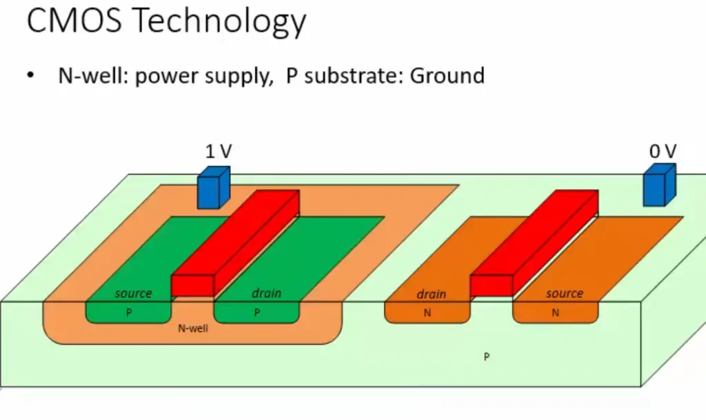
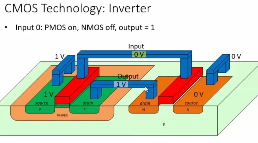
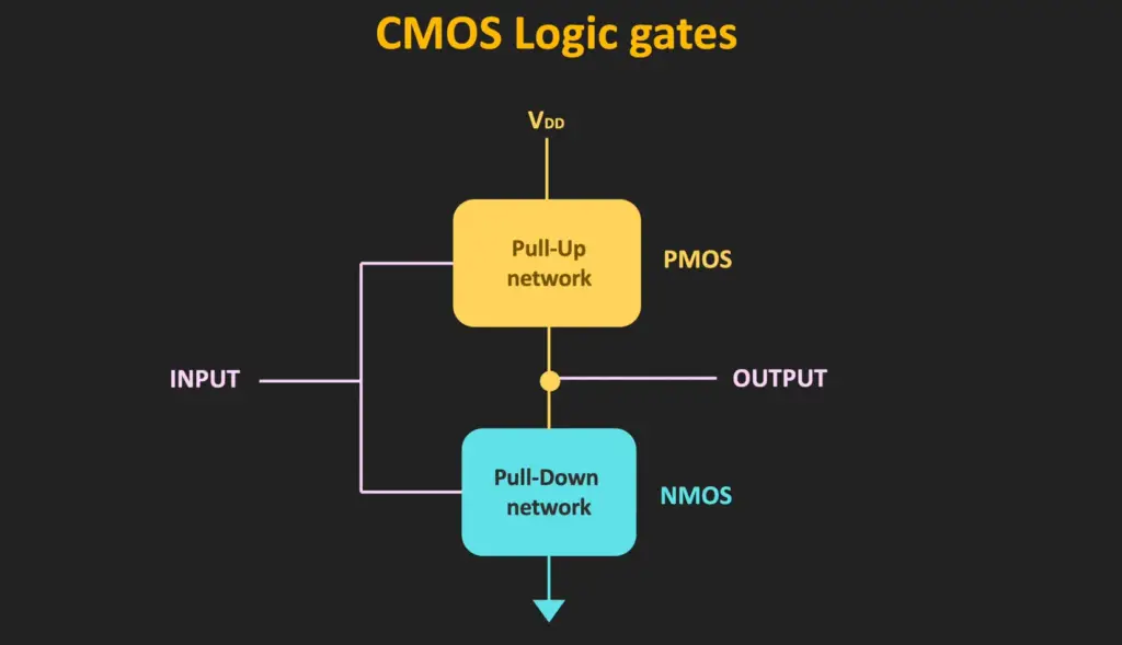
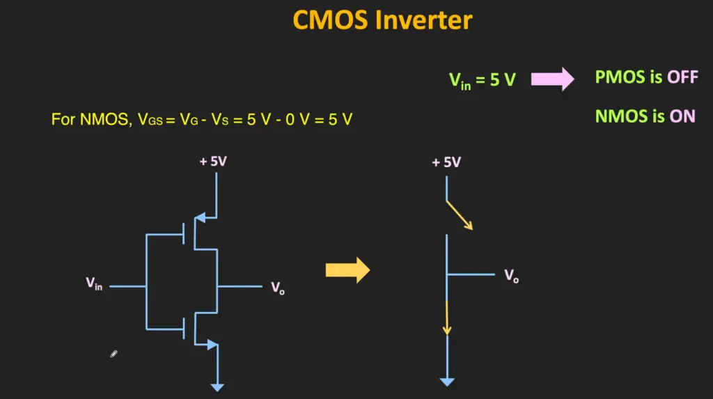
The fundamental operation of a CMOS inverter is based on the two transistors, namely p-type and n-type MOSFETs in a complementary arrangement. The two transistors are either in cut-off or saturation regions depending on the input logic level. When the input voltage is high (logic 1), the pMOS transistor will be turned off and the nMOS transistor will turn on to allow current flow from output to ground. This condition at the output terminal results in a low voltage or logic 0 state. On the other hand when the input voltage is low (logic 0), then the nMOS transistor turns off and no current flows through it resulting in a high voltage or logic1 state at the output terminal.
The two transistors built in a CMOS inverter are cross-coupled, meaning they are linked to each other’s gate inputs. One transistor is used as a switch and the other one does the opposite job of maintaining its resistance high when the first transistor is off. This device structure has several advantages over other discrete logic designs including low power consumption and noise immunity due to its symmetrical design. The input voltage range for a CMOS inverter can be from 0-5V with an acceptable noise margin of 1.5V on either side at room temperature, making it suitable for digital applications like microprocessors or memory circuits where low power consumption is desired. [1], [2]
CMOS Inverter Characteristics
CMOS inverters are characterized by a few parameters that define their behavior. These characteristics include its power supply voltage, propagation delay, noise margin, output current and fan-out. Besides those, there are two characteristics you want to consider.
Inverter Static Characteristics or VTC
The static characteristics of a CMOS inverter are determined by the voltage transfer characteristic (VTC), also known as an I-V curve. This graph shows how the output responds to different input levels.
An ideal CMOS inverter will have a symmetric VTC with a steep slope near the middle of its range, which is known as the switching point. The switching point is when the output changes from high to low or vice versa, depending on the input level.
The VTC or voltage transfer curve resembles an inverted step function that specifies switching between the two possible output states when the input crosses the switching point. The voltage transfer curve highlights that when the input voltage (Vin) is low, the circuit produces a high output voltage (Vout), while if Vin is large, Vout equals 0 volts.
The transition region slope is a measure of quality – steep slopes yield exact switching. The tolerance toward noise can be calculated by evaluating the smallest input to the highest output for every region of ON or OFF operation.
Inverter Dynamic Characteristics
The dynamic characteristics of a CMOS inverter include different parameters, such as its switching threshold voltage and rise/fall times.
Fall times refer to the time it takes for the voltage at the output to drop from its high level to its low level, while rise times refer to the time it takes for the voltage at the output to rise from its low level to its high level.
Contamination delay is another important dynamic characteristic of a CMOS inverter. This refers to the delay caused due to contamination, such as dust or oxidation on the metal layer of an integrated circuit.
CMOS Inverter Applications
CMOS inverters have a wide range of applications in digital electronics. They are used extensively in logic circuits, memory cells, power supply control and signal decoding. In this section we will discuss some of the most common applications of CMOS inverters.
Different ICs
CMOS inverters are available in different IC (integrated circuit) packages. The most common package types are dual-in-line package or DIP, small-outline integrated circuit or SOIC and plastic leaded chip carrier or PLCC. Each of these packages has its own advantages and drawbacks depending on the application.
The DIP package is the most common for prototyping CMOS circuits due to its low cost and easy to use pinouts. It also provides more flexibility when it comes to routing connections between components due to its wider pins compared with other IC packages. On the downside, it is more prone to damage from mishandling because it does not have any protection features such as a lid or case like some other
Mobile devices
CMOS inverters are commonly used as switches in mobile devices such as smartphones and tablets. The small size and low power consumption of CMOS inverters make them ideal for use in these types of devices where battery life is a priority. They typically control the power supply to various components, allowing the device to remain powered off when not in use and conserve battery life.
Digital cameras
CMOS inverters are used in digital cameras to enable the transmission of data from the imaging sensor chip to the camera processor. The CMOS inverter is responsible for converting analog signals into digital signals, which can then be processed by the camera’s processor. [1], [2]
Advantages of CMOS Inverters (detailed answer
CMOS inverters offer several advantages over other types of logic gates. Let’s discuss all the advantages of CMOS inverters.
Negligible steady-state power dissipation
It is generally measured in watts (W) and is an important factor when it comes to the design, operation, and maintenance of electrical systems.
The most significant advantage of CMOS inverters is their negligible power dissipation in steady-state conditions. This means that the circuit does not require any external power source, resulting in a very low standby power consumption when compared to other logic gates.
Low power consumption
The great advantage of CMOS inverters is their low power consumption. Since the transistors are only active when switching between High and Low states, they consume very little power compared to other types of logic circuits. This makes them ideal for portable devices where battery life is important.
High noise immunity
In addition to their low power consumption, CMOS inverters also have a high noise immunity due to the fact that voltage levels do not need to be as precisely controlled in comparison with other logic gate designs.
High noise immunity is the ability of a CMOS inverter to resist electrical interference from outside sources, such as nearby electronic devices or high voltage power lines. A CMOS inverter will usually have a higher noise immunity than other types of digital circuits such as TTL, DTL and ECL. Noise immunity is achieved by having an input signal which needs to stay within certain voltage limits before it can be accepted as valid (known as hysteresis). This process helps reduce errors in the circuit caused by small fluctuations in the input signal.
Low cost mass production
CMOS inverters are much cheaper to produce in large quantities compared to other logic gates. This is due to the fact that they are usually made with standard MOSFETs, which can be found in abundance and cheaply mass-produced.
The low cost of production also allows CMOS inverters to be used in a wide range of applications from consumer electronics to industrial automation. They are an ideal choice for circuits where budget is a priority, as well as for hobbyists looking for cheap solutions.
Exhibit a complete o/p voltage swing in between 0 V & VDD
Another advantage of CMOS inverters is that they exhibit a complete output voltage swing in between 0 V and the power supply voltage (VDD). This means that they can be used to produce a variety of analogue waveforms, ranging from sine waves to square waves. These waveforms are essential for many applications, including oscillators and amplifiers.
By comparison, other logic gates such as TTL or DTL have limited output swings which may not be sufficient for certain tasks. This makes CMOS inverters an ideal choice when precision is required.
The CMOS inverter is designed to exhibit a complete output voltage swing in between 0 V and VDD, which means that the voltage level at the output terminal can range from 0 V to ground and up to VDD. This allows for higher speed operation and also improves noise immunity. [1]
Disadvantages of CMOS Inverters
CMOS inverters have a few drawbacks that should be taken into consideration when designing circuits. It’s important to be aware of the disadvantages of CMOS inverters to ensure your circuit is safe and reliable.
High switching speed
One of the primary disadvantages of CMOS inverters is their high switching speed. This can cause interference with other circuits and result in glitches or less than optimal performance. The high switching speed also makes it harder to troubleshoot any issues that may arise, as it takes longer to detect them. Additionally, the power consumption can increase due to the increased frequency of operation.
Difficult to fabricate
CMOS inverters are very difficult to fabricate, since the components used in them require a high level of precision. This can make it difficult to scale up production and achieve consistent results between individual chips.
Additionally, any slight imperfections in the fabrication process could cause short circuits or other undesired effects, making even small mistakes expensive and time-consuming to fix.
Requires more space
Because it needs two transistors and associated circuitry, a CMOS inverter requires more space than other types of logic gates. This can be a limiting factor in applications where space is at a premium, such as on an IC chip or PCB. Additionally, the extra components and circuitry consume more power than other types of logic gates, which can have implications for battery powered devices.
This is especially true when compared to TTL inverters which only require one transistor and minimal additional components. The increased footprint can be a major concern in circuit designs with limited board space. [1]
FAQ
What is the main disadvantage of a CMOS inverter?
The biggest disadvantage of CMOS inverters is their big size. Due to the need for additional transistors, capacitors, and other components, a CMOS inverter will generally require more real estate than its TTL counterparts. Additionally, due to their increased complexity, they are typically also more expensive than TTL inverters.
What is the CMOS inverter explanation?
When the input voltage applied to the gate of the transistor exceeds the threshold voltage, current flows through the circuit, allowing for digital signals with values of either “high” or “low” to be transmitted. The output signal obtained from a CMOS inverter is always opposite to that of its input signal – it inverts. This makes it ideal for use in digital circuits where signals need to be inverted or otherwise processed by complementary logic gates.
What are the two advantages of a CMOS inverter?
A CMOS inverter has several advantages over other logic gates. The most notable are its low power consumption and noise immunity.
The low power consumption of a CMOS inverter is due to the fact that it switches between two different states without passing through an intermediate state, meaning that it only requires very minimal current to switch between those two different states. This makes them ideal for applications where battery life is important or energy efficiency is required.
Another advantage of the CMOS inverter is its high noise immunity. This means that it can reject any external interference from outside sources such as electromagnetic fields or radio signals, allowing it to remain functional even in environments with significant electrical noise levels. As a result, they are often used in critical applications where a standard logic gate would be too vulnerable to interference.
What are CMOS inverter characteristics?
CMOS inverters are electronic circuits that form the basis of all digital logic. They take an input, usually a voltage or current, and output a digital signal representing the inverse of the input. This can be used to create a wide variety of logic functions including AND, OR, NAND, NOR, NOT and XOR gates as well as many other combinations. The key characteristics of CMOS inverters include:
- Low power consumption: CMOS transistors require very low power for their operation; this makes them ideal for battery powered systems where high efficiency is important.
- High input impedance: CMOS transistors have a very high input impedance; this makes them suitable for driving large loads without significantly loading down the signal source.
- Wide voltage range operation: CMOS transistors can operate over a wide voltage range, making them suitable for applications with fluctuating supply voltages.
What does the CMOS inverter consist of?
The CMOS inverter is a basic logic gate, and as such, it consists of two transistors. One transistor acts as an input device while the second one works as an output device. The input transistor is responsible for taking the input value (either HIGH or LOW) and passing it to the output transistor. When the input signal is HIGH, then the output signal will be LOW, and vice versa. This type of circuit is known as an Inverter because it inverts (or switches) between high and low values.
In addition to these two transistors, there are other components involved in a CMOS inverter such as resistors or capacitors which help adjust power levels or provide additional filtering functions. All these components work together to form a complete CMOS inverter circuit.
Useful Video: CMOS Tech: NMOS and PMOS Transistors in CMOS Inverter (3-D View)
Conclusion
CMOS Inverters are an important tool for digital logic design. They are versatile, robust, and user friendly components used to make reliable logic circuits. When correctly designed they offer low-power operation while maintaining high performance characteristics. This makes them attractive to designers of all levels of experience in the field of electronics engineering.
Using CMOS Inverters can help you build efficient and powerful digital circuits that perform better than many other types of inverters. As you found out during this guide, there are different types of CMOS Inverters available on the market such as voltage transfer ratio, power supply requirements, rise/fall times, hysteresis properties, and packaging options. All these parameters need to be considered when choosing a particular type depending on your application.
To wrap up, a CMOS Inverter is a versatile and robust component that can be used to create compact and reliable logic circuits. It offers low power operation while maintaining high performance characteristics. Furthermore, it has different types of options available on the market in order to better suit the requirements of your design. With the right knowledge and understanding, you should have no problems designing logic circuits with CMOS Inverters.
Before starting any project with a CMOS inverter it’s important to take into consideration all the parameters involved such as voltage transfer ratio, power supply requirements, rise/fall times, hysteresis properties, and packaging options before making a final decision about which type of inverter to use. Furthermore, the best way to ensure a successful design is to use reliable and tested components that meet the required specifications of your project. Following these practices will ensure you get the most out of CMOS Inverters for all your digital logic design needs.
We hope this guide has been helpful in understanding what a CMOS inverter is and how it can be used in digital logic designs. Good luck and happy designing!
References
- https://www.elprocus.com/cmos-inverter/
- https://byjusexamprep.com/cmos-inverter-i