
The pinch-off voltage is a fundamental parameter in the operation of Junction Field-Effect Transistors (JFETs) that plays a crucial role in controlling current flow through the device. Understanding the concept of pinch-off voltage is essential for engineers and electronics enthusiasts working with JFETs.
In this article, we will explore in detail what the pinch-off voltage is, how it is determined, its significance in JFET operation, and the implications it has on circuit design and analysis. By grasping the concept of the pinch-off voltage, readers will gain a deeper understanding of the behavior and characteristics of JFETs.
JFET Definition And Guide:
History
The JFET was invented by Julius Edgar Lilienfeld in 1925, although it was not until the 1960s that it gained practical significance. Following Lilienfeld’s initial work, other scientists and engineers further developed and refined the JFET’s design, leading to its widespread use in various electronic applications [1].
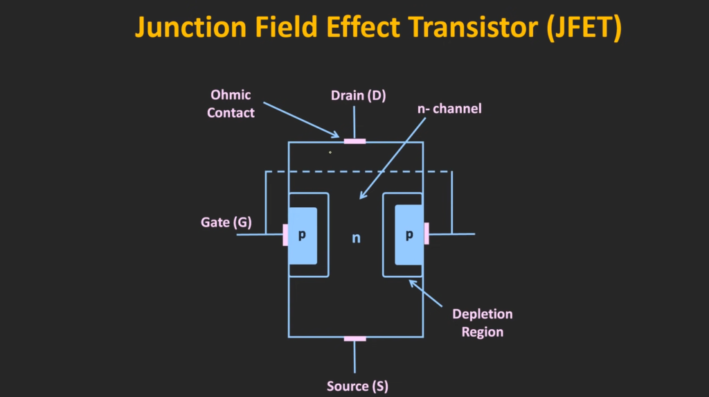
Structure
Functions
The JFET operates based on the principle of electric field control. By applying a voltage to the gate terminal, the electric field between the gate and the channel is altered, which affects the current flow through the channel. The JFET can function as either an n-channel or p-channel device, depending on the doping of the semiconductor material.
Schematic Symbols
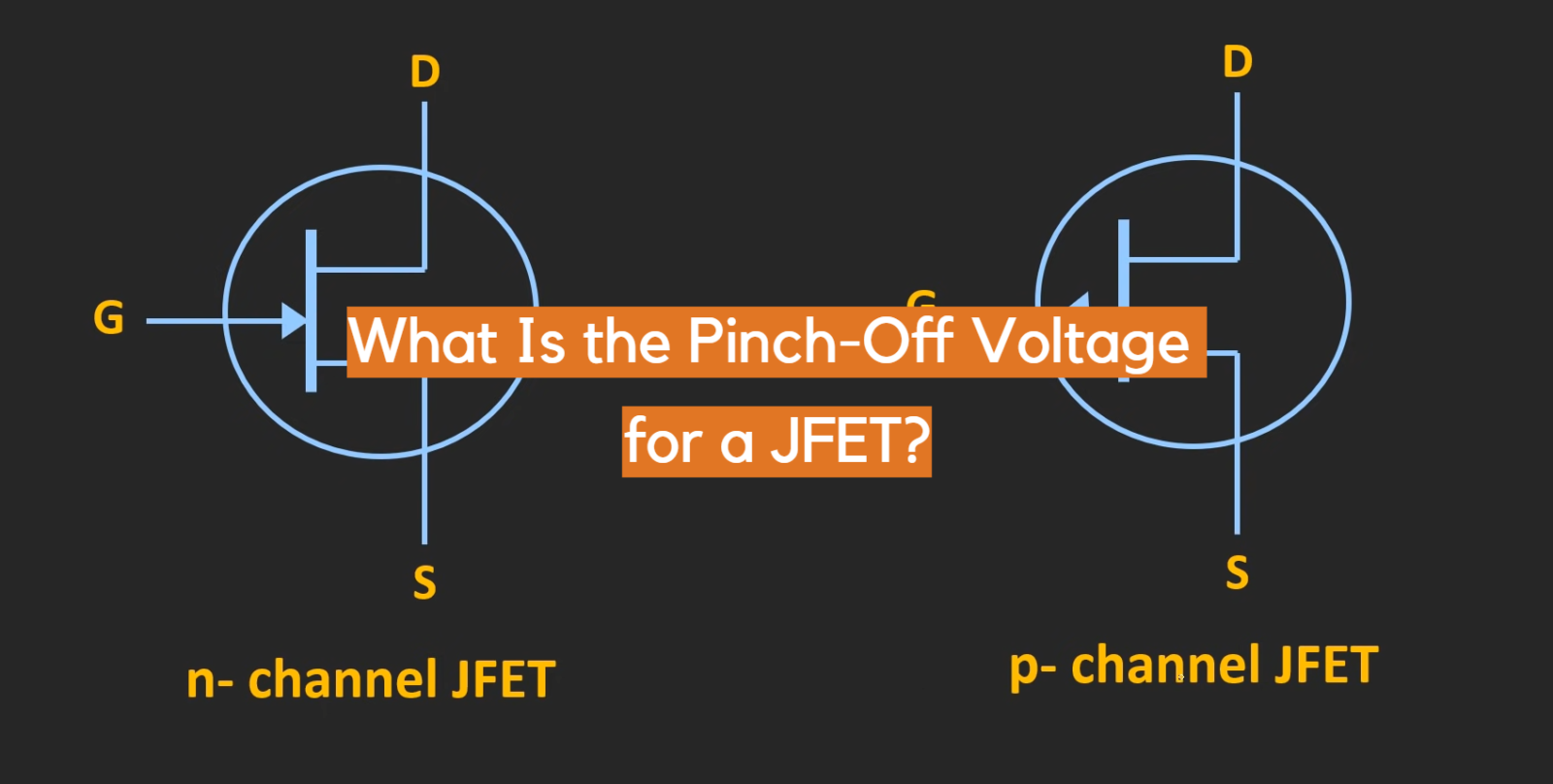
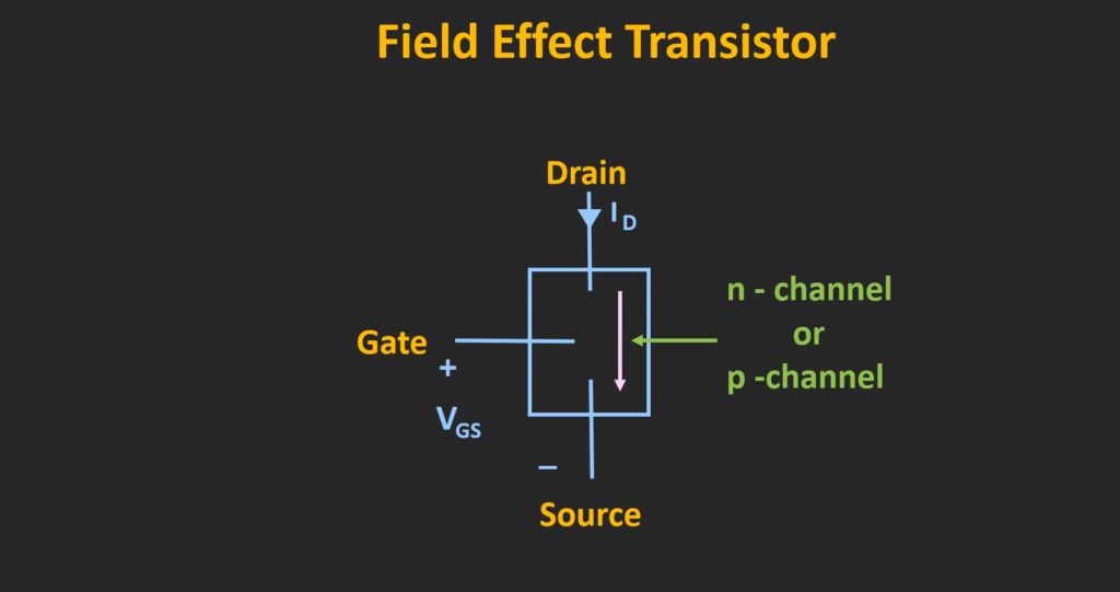
To represent a JFET in electronic circuits, specific schematic symbols are used. The symbol for an n-channel JFET resembles an arrow pointing inward, while the symbol for a p-channel JFET resembles an arrow pointing outward. These symbols are essential for circuit designers to accurately depict JFETs in their circuit diagrams.
Comparison With Other Transistors
JFETs are distinct from other types of transistors such as bipolar junction transistors (BJTs) and metal-oxide-semiconductor field-effect transistors (MOSFETs). While BJTs are current-controlled devices and MOSFETs are voltage-controlled devices, JFETs operate based on the control of electric fields. JFETs typically have high input impedance, low noise, and excellent high-frequency characteristics, making them suitable for specific applications.
Mathematical Model
The behavior of JFETs can be mathematically modeled to understand their operation more precisely. The most commonly used model is the square-law model, which describes the relationship between the input voltage (Vgs) and the drain current (Ids). This model assumes that the drain current is proportional to the square of the input voltage [2].
Linear Ohmic Region
In the linear ohmic region, the JFET operates as a variable resistor, allowing current to flow relatively freely through the channel. In this region, the drain current is directly proportional to the gate-to-source voltage, and the JFET acts as a voltage-controlled resistor.
Constant-Current Region
Beyond the linear ohmic region, the JFET enters the constant-current region. Here, the drain current remains relatively constant, regardless of changes in the gate-to-source voltage. This region is particularly useful for applications that require a stable current source.
Transconductance
Transconductance (gm) is a crucial parameter that measures the change in drain current with respect to changes in the gate-to-source voltage. It indicates the amplification capability of the JFET and determines its performance in various applications. The higher the transconductance, the greater the amplification potential.
How a JFET Works:
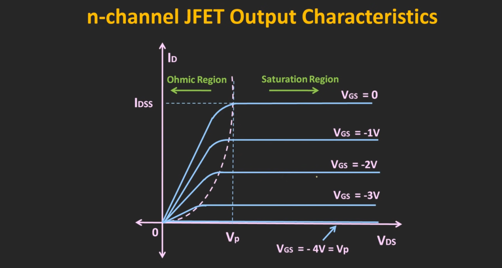
Output Characteristics
The output characteristics of a JFET illustrate the relationship between the drain current (ID) and the drain-source voltage (VDS). These characteristics help us understand how the JFET behaves under different operating conditions. The output curve typically displays a linear region followed by a saturation region.
Transconductance Characteristics
Transconductance (gm) is a crucial parameter that defines the amplification capability of a JFET. It measures the change in drain current (ID) with respect to the change in the gate-source voltage (VGS). The transconductance characteristics show how the JFET responds to different input voltages, indicating its amplification potential.
Operation
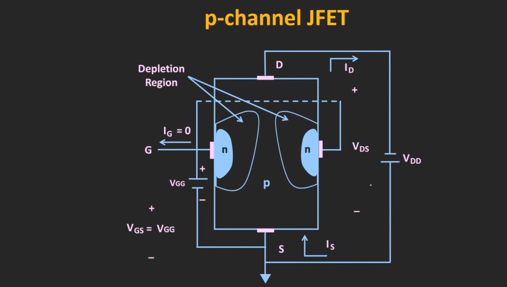
The operation of a JFET is based on the control of the electric field within the channel region. When a voltage is applied to the gate-source junction, it modifies the depletion region’s width, altering the current flow through the channel. This control mechanism allows the JFET to act as a voltage-controlled device.
Voltage Controlled Transistor
The JFET is often referred to as a voltage-controlled transistor due to its behavior. Unlike the bipolar junction transistor (BJT), which is a current-controlled device, the JFET relies on the voltage applied to the gate-source terminal to regulate the current flow. This property makes the JFET suitable for specific applications where voltage control is desired.
About The Pinch-Off Voltage
The pinch-off voltage (VP) is a critical parameter in JFET operation. It refers to the gate-source voltage at which the channel conduction is significantly reduced, restricting the current flow. At this voltage, the depletion region expands, and the channel becomes narrower, leading to the pinching off of the current path. The pinch-off voltage is an important parameter to consider in JFET design and circuit analysis.
Operation Below “Pinch-Off”
When operating a JFET below the pinch-off region, the gate-source voltage is lower than the pinch-off voltage (VGS < VP). In this region, the channel is open, and the JFET acts as a variable resistor. The drain current is directly proportional to the gate-source voltage, and the JFET exhibits voltage-controlled resistance behavior. This region is useful for applications that require voltage amplification or variable resistance.
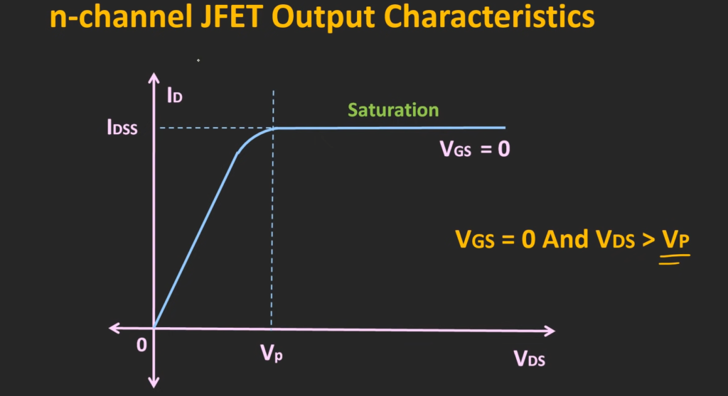
Operation Above “Pinch-Off”
Operating a JFET above the pinch-off region involves applying a gate-source voltage higher than the pinch-off voltage (VGS > VP). In this region, the channel is pinched off, and the JFET acts as a constant-current device. The drain current remains relatively constant, regardless of changes in the drain-source voltage (VDS). This region is suitable for applications that require a stable current source.
How Is The Pinch Off Voltage Calculated?
For a Junction Field Effect Transistor (JFET), the pinch-off voltage can be calculated by using the following formula:
Vp = -IDSS / (2 x IDOFF x [1 – (VP/VP0)^1/2 ])
Where Vp is the pinch-off voltage, IDSS is the saturation current, IDOFF is the drain current with the gate shorted to the source, VP0 is the zero-bias pinch-off voltage, and ^1/2 indicates the square root function [3].
For a Metal-Semiconductor Field-Effect Transistor (MESFET), the pinch-off voltage can be calculated using the following formula:
VP = Eb – (VT + 2Φf)/g
Where VP is the pinch-off voltage, Eb is the barrier energy for the gate, VT is the thermal voltage, Φf is the Schottky barrier, and g is the transconductance.
It’s worth noting that these formulas are just a starting point. The actual pinch-off voltage will depend on various factors, including the physical characteristics of the transistor and the specific operating conditions.
What Is The Pinch-Off Voltage For A JFET?
The pinch-off voltage for a Junction Field Effect Transistor (JFET) is the drain-to-source voltage at which the drain current becomes almost constant and the transistor enters the pinch-off region.
In other words, it is the voltage at which the channel between the source and drain is pinched off, making it almost constant, and the transistor turns off. The actual value of the pinch-off voltage depends on the specific characteristics and operating conditions of the JFET.
It can be calculated using the formula Vp = -IDSS / (2 x IDOFF x [1 – (VP/VP0)^1/2 ]), where Vp is the pinch-off voltage, IDSS is the saturation current, IDOFF is the drain current with the gate shorted to the source, VP0 is the zero-bias pinch-off voltage, and ^1/2 indicates the square root function [4].
FAQ:
1. How is the pinch-off voltage for a JFET determined?
The pinch-off voltage (VP) for a JFET is typically determined during the fabrication process. It is influenced by the doping concentration and the physical dimensions of the JFET’s channel region. The specific values of VP are determined by the semiconductor material and the manufacturing parameters used in the JFET production.
2. What is the formula for FET pinch-off voltage?
The formula for the pinch-off voltage of a JFET is generally not a simple mathematical equation. It is primarily determined during the device fabrication process and is influenced by various factors such as doping concentration, channel dimensions, and manufacturing parameters. Therefore, there is no specific formula to calculate the pinch-off voltage.
3. What is the difference between pinch-off voltage and cut-off voltage in JFET?
In JFETs, the pinch-off voltage (VP) refers to the gate-source voltage at which the channel conduction is significantly reduced, leading to a restricted current flow. It represents the voltage level at which the JFET enters the constant-current region [5].
On the other hand, the cut-off voltage (VGS(off)) refers to the gate-source voltage at which the drain current is effectively zero, and the JFET is turned off. While both voltages have different implications, they both relate to the control of current flow in the JFET.
4. What is the effect of the pinch-off voltage?
The pinch-off voltage is a crucial parameter in JFET operation as it determines the point at which the channel conduction is significantly reduced. It affects the overall behavior of the JFET by defining the transition between the linear ohmic region and the constant-current region. The pinch-off voltage helps regulate the current flow through the channel and allows for voltage-controlled resistance or constant-current operation.
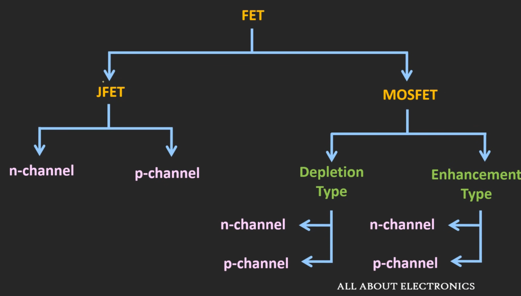
5. What is the difference between JFET and MOSFET?
The main difference between JFETs and Metal-Oxide-Semiconductor Field-Effect Transistors (MOSFETs) lies in their construction and operation. JFETs are typically made of a doped semiconductor material and are voltage-controlled devices. They have a simple structure with a single-channel and operate in either an n-channel or p-channel configuration.
In contrast, MOSFETs utilize an insulated gate structure, with a metal oxide layer acting as a gate dielectric. MOSFETs are voltage-controlled devices as well, but they offer greater versatility and are widely used in modern integrated circuits.
6. Why is FET voltage controlled?
FETs, including both JFETs and MOSFETs, are voltage-controlled devices because their output characteristics and behavior depend on the voltage applied to the gate terminal. By adjusting the gate voltage, the electric field in the channel region is altered, leading to changes in the conductivity and current flow. This voltage-controlled behavior allows for precise control and modulation of the output current.
7. Why is JFET voltage controlled?
Similar to other FETs, JFETs are voltage-controlled devices because their operation is primarily based on the voltage applied to the gate terminal. The voltage at the gate modulates the electric field within the channel, influencing the channel’s resistance and controlling the current flow. This voltage-controlled behavior makes JFETs suitable for applications requiring precise voltage control and amplification.
8. What is VP in JFET?
VP, also known as the pinch-off voltage, refers to the gate-source voltage at which the channel conduction in a JFET is significantly reduced. It represents the voltage level at which the JFET enters the constant-current region. VP determines the point at which the channel is effectively pinched off, restricting the current flow through the device.
9. Why is pinch-off voltage negative?
The pinch-off voltage in JFETs is typically negative due to the n-channel or p-channel configuration of the device. In an n-channel JFET, the pinch-off voltage is negative with respect to the source terminal. In a p-channel JFET, the pinch-off voltage is positive with respect to the source terminal. The polarity of the pinch-off voltage is determined by the doping of the semiconductor material used in the JFET.
10. What is VGS in a JFET?
VGS refers to the gate-source voltage in a JFET. It represents the voltage difference between the gate and source terminals. The VGS determines the electric field in the channel region, thereby controlling the current flow through the JFET.
11. Does JFET have high voltage gain?
JFETs are typically known for their high input impedance and low output impedance, making them suitable for voltage amplification applications. However, JFETs on their own do not offer high voltage gain compared to other amplification devices. To achieve higher voltage gain, additional amplification stages or configurations, such as cascode or common-source amplifier configurations, can be employed using JFETs.
12. Why use FET over BJT?
FETs, including JFETs and MOSFETs, offer certain advantages over Bipolar Junction Transistors (BJTs). FETs have a higher input impedance, which reduces loading effects on input circuits. They also have a faster switching speed, making them suitable for high-frequency applications.
Additionally, FETs operate with lower power consumption and exhibit less noise compared to BJTs. However, BJTs are often preferred in low-voltage, high-current applications and when precise current control is required.
13. What are the two types of JFET?
JFETs can be classified into two types based on the doping of the channel region: n-channel JFETs and p-channel JFETs. In an n-channel JFET, the channel region is doped with a donor impurity, resulting in an excess of free electrons. In a p-channel JFET, the channel region is doped with an acceptor impurity, creating a deficiency of free electrons and an excess of holes.
14. Who invented JFET?
The JFET was initially invented by Julius Edgar Lilienfeld in 1925. However, Lilienfeld’s original patents and work did not gain practical significance at that time. Subsequent development and refinement of the JFET by other scientists and engineers, including William Shockley, led to its practical implementation in electronic applications.
15. What causes the pinch-off voltage?
The pinch-off voltage in a JFET is caused by the control of the depletion region’s width within the channel region. When the gate-source voltage reaches a certain level, the depletion region expands, effectively reducing the width of the channel and restricting the current flow. This phenomenon leads to the pinch-off effect and defines the pinch-off voltage of the JFET.
16. Which MOSFET is normally off?
Enhancement-mode MOSFETs are normally off devices. In enhancement-mode MOSFETs, no channel exists between the source and drain terminals without the application of a voltage at the gate terminal. They require a positive gate-source voltage to create a conducting channel and allow current flow.
17. What is threshold voltage and pinch-off voltage?
Threshold voltage (Vth) and pinch-off voltage (VP) are related but distinct parameters in FETs. The threshold voltage refers to the gate-source voltage at which the FET just starts to conduct. It represents the voltage level at which the FET transitions from the off state to the on state.
On the other hand, the pinch-off voltage represents the gate-source voltage at which the channel conduction is significantly reduced, leading to a restricted current flow. It defines the point at which the FET enters the constant-current region.
18. What are the features of JFET?
Some key features of JFETs include:
- High input impedance: JFETs offer high input impedance, making them suitable for circuits requiring minimal loading effects on input signals;
- Low noise: JFETs exhibit low noise characteristics, making them advantageous in low-noise amplifier circuits;
- Simple structure: JFETs have a relatively simple structure, consisting of a single channel and three terminals (source, gate, and drain);
- Voltage-controlled device: JFETs are voltage-controlled devices, relying on the voltage applied to the gate terminal to regulate current flow;
- Suitable for high-impedance applications: Due to their high input impedance, JFETs are commonly used in circuits that require high-impedance input stages;
19. How does JFET work as an amplifier?
JFETs can work as amplifiers by utilizing their voltage-controlled resistance behavior. In a common-source configuration, a small input voltage applied at the gate terminal can control the current flowing through the channel, resulting in an amplified output voltage at the drain terminal. By adjusting the gate-source voltage, the JFET can modulate the output signal and provide amplification.
20. What is the difference between JFET and BJT?
The main differences between JFETs and BJTs include:
- Control mechanism: JFETs are voltage-controlled devices, whereas BJTs are current-controlled devices;
- Input impedance: JFETs offer higher input impedance compared to BJTs, which can reduce loading effects on input circuits;
- Output impedance: BJTs typically have lower output impedance compared to JFETs;
- Amplification types: JFETs are primarily used for voltage amplification, while BJTs are commonly employed for current amplification;
- Polarity: JFETs can have either n-channel or p-channel configurations, while BJTs are available in either NPN or PNP configurations;
21. What is the depletion mode of JFET?
The depletion mode of a JFET refers to the condition where the channel is already established even with zero applied voltage at the gate terminal. In this mode, the channel is present in the absence of an external gate-source voltage, and the JFET is in an “on” state by default. Depletion-mode JFETs are less commonly used compared to the more prevalent enhancement-mode JFETs.
Useful Video: JFET: Construction and Working Explained
References
- https://learnabout-electronics.org/Semiconductors/fet_02a.php
- https://www.etechnog.com/2022/01/what-is-pinch-off-voltage-explained.html
- https://electrotopic.com/what-is-the-pinch-off-voltage-for-a-jfet/
- https://en.wikipedia.org/wiki/JFET
- https://www.ee.columbia.edu/~bbathula/courses/SSDT/lect11.pdf