Printed Circuit Boards (PCBs) are the backbone of modern electronics, serving as a platform for interconnecting electronic components. PCBs provide a compact, cost-effective, and reliable way to create electronic circuits.
A fundamental element of any PCB is the via, which is an essential component for routing electrical signals between different layers of a PCB. Vias come in different shapes, sizes, and types, depending on the design requirements and the manufacturing process.
The via is lined with a conductive material that allows current to flow through the board, providing a connection between the different layers. The use of vias in PCB design is an essential technique that enables designers to create more compact and sophisticated circuits while maintaining high levels of functionality.
Without vias, PCBs would require more layers, taking up more space and becoming more expensive to manufacture. In modern electronics, where miniaturization is a primary concern, vias have become a crucial tool for designers to create smaller, more efficient, and cost-effective electronic devices.
In this article, we will explore what vias are, their types, how they are created, and their applications. We will also delve into the factors that designers must consider when creating vias to ensure they meet the specific requirements of their applications. By the end of this article, you will have a clear understanding of the importance of vias in PCB design and the critical role they play in the functionality of modern electronic devices.
What Is a Via?
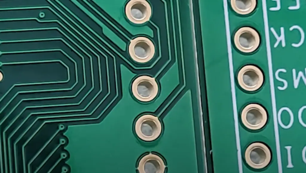
Vias come in different shapes, sizes, and types, depending on the design requirements and the manufacturing process. The most common type of via is a plated-through via, which is formed by drilling a hole through the entire board and then plating the walls of the hole with a conductive material.
This creates a metal-plated tunnel that connects the conductive layers of the PCB. Non-plated vias, on the other hand, are holes that are not plated and are used to create through-hole connections for components or to provide a path for test probes. Understanding the role of vias in PCB design is crucial for creating functional and reliable electronic circuits.
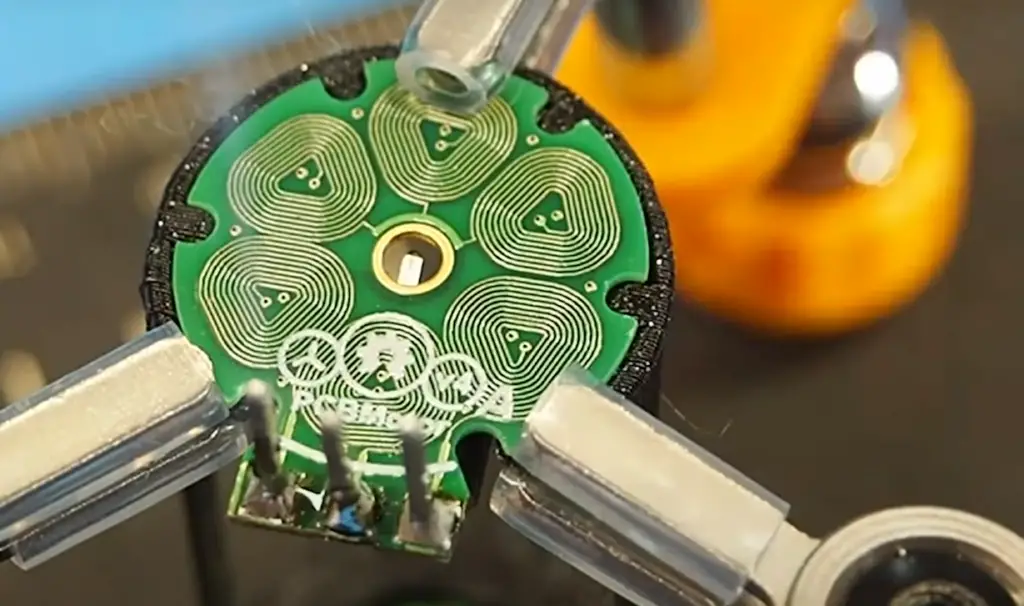
What Is the Role of Via in PCB?
The primary function of a via is to establish an electrical connection between the different layers of a PCB. Vias allow electrical signals to travel vertically through the board, connecting the conductive traces on different layers. Vias also allow components to be placed on both sides of the PCB, making it possible to create more complex circuits in a smaller space.
In a multi-layer PCB, vias allow signals to travel through the board vertically, connecting the conductive traces on different layers. Furthermore, vias can be used to dissipate heat generated by components on the board, as they provide a path for heat to flow from one layer to another.
How Can Vias Impact PCB Design?
One of the main ways that vias can impact PCB design is through their effect on signal integrity. Vias can create impedance mismatches and signal reflections, leading to data errors, noise, and reduced signal quality. The use of blind or buried vias, which do not extend through the entire thickness of the board, can help to minimize these effects, but they can also add complexity and cost to the design.
Vias can also impact the thermal management of a PCB. The placement of vias can affect the flow of heat within the board, and the size and density of vias can impact the ability of the board to dissipate heat. In high-power applications, it may be necessary to use thermal vias to improve heat dissipation and prevent hot spots.
Finally, the physical design of vias can impact the reliability and manufacturability of a PCB. For example, small vias may be more prone to electroplating issues, and improperly designed or placed vias can create stress points that can lead to cracking or delamination of the board.
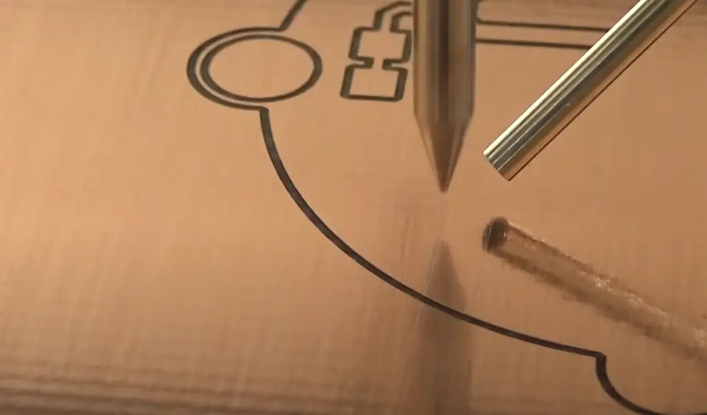
Components Of Via In PCB:
Barrel
It is the most critical component of the via, as it establishes the electrical connection between the different layers of the PCB. The diameter of the barrel is determined by the size of the drill used to make the via. The diameter of the barrel should be large enough to allow the necessary current to flow through it without causing excessive resistance, but not so large that it takes up too much space on the board [2].
The thickness of the barrel walls is also important. The thickness of the barrel walls should be enough to provide adequate mechanical support for the via, but not so thick that it takes up too much space on the board. The thickness of the barrel walls is typically determined by the manufacturing process and the materials used.
The quality of the plating on the barrel walls is also critical. The plating should be thick enough to provide a reliable electrical connection between the layers of the PCB. The plating should also be uniform and free of voids, cracks, or other defects that could compromise the integrity of the via.
Pad
The purpose of the pad is to provide a stable and reliable connection between the via and the components on the board. The size and shape of the pad depending on the size of the component that will be connected to the via.
The pad diameter should be large enough to provide a stable connection between the via and the component, but not so large that it takes up too much space on the board. The pad should also be placed in a location that allows for easy access to the component.
The quality of the plating on the pad is also important. The plating should be thick enough to provide a reliable electrical connection between the via and the component. The plating should also be uniform and free of voids, cracks, or other defects that could compromise the integrity of the via.
Antipad
The purpose of the antipad is to prevent the conductive pad from shorting to other conductive elements on the board, such as other vias or traces. The size and shape of the antipad depend on the size and shape of the pad.
The antipad diameter should be large enough to prevent the pad from shorting to other conductive elements on the board, but not so large that it takes up too much space on the board. The antipad should also be placed in a location that prevents it from overlapping with other conductive elements on the board [3].
The distance between the pad and the antipad is also critical. The distance should be large enough to prevent the pad from shorting to other conductive elements on the board, but not so large that it takes up too much space on the board.
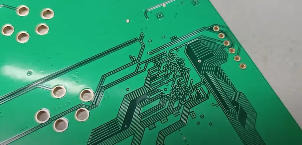
Important Considerations About Vias:
Aspect Ratio
The aspect ratio of a via is the ratio of the diameter of the via to its depth. The aspect ratio is a critical factor in determining the reliability of the via. If the aspect ratio is too high, the via may not be able to withstand the stresses of the manufacturing process or the thermal cycles of the circuit’s operation. Conversely, if the aspect ratio is too low, the via may not provide a reliable connection between the layers of the PCB.
The aspect ratio of a via depends on several factors, including the diameter of the via, the thickness of the PCB, and the materials used in the manufacturing process. The aspect ratio should be carefully considered during the design phase to ensure that the via will be reliable and able to withstand the stresses of the manufacturing process and the circuit’s operation.
Annular Ring
The annular ring is critical for providing a stable and reliable connection between the via and the components on the board. The size of the annular ring depends on several factors, including the diameter of the via and the size of the component that will be connected to the via.
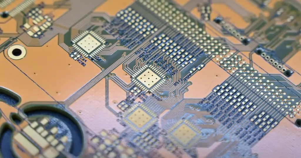
The size of the annular ring should be carefully considered during the design phase to ensure that it provides a stable and reliable connection between the via and the component. If the annular ring is too small, the connection may not be stable, and if it is too large, it may take up too much space on the board.
Signal Integrity
Signal integrity is a critical consideration in PCB design, and vias play a significant role in signal integrity. Vias can affect the electrical performance of the circuit by introducing impedance, capacitance, and inductance. The impact of vias on signal integrity depends on several factors, including the size of the via, the distance between the vias, and the materials used in the manufacturing process.
The impact of vias on signal integrity can be reduced by using high-quality materials, minimizing the distance between the vias, and carefully controlling the via size and aspect ratio. Simulation tools can also be used to analyze the impact of vias on signal integrity and optimize the design for the best possible electrical performance.
Routing Density
The routing density can affect the reliability and performance of vias. If the routing density is too high, the vias may not be able to handle the necessary current or may not provide a reliable connection between the layers of the PCB. Conversely, if the routing density is too low, it may not be possible to route all the necessary traces through the board [4].
The routing density should be carefully considered during the design phase to ensure that the vias can handle the necessary current and provide a reliable connection between the layers of the PCB. If the routing density is too high, additional vias may need to be added to the design, and if it is too low, the design may need to be simplified or made larger to accommodate the necessary traces.
Benefits of Vias:
Signal Routing
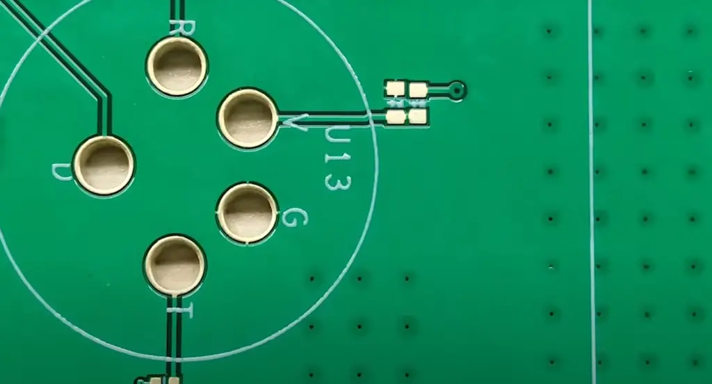
Vias offer significant advantages in signal routing for PCB design. They enable designers to connect signal traces between layers, facilitating high-speed data transmission between components. Additionally, vias allow for closer component placement, leading to a smaller PCB footprint and improved device performance.
Furthermore, vias can enhance signal integrity by mitigating electromagnetic interference (EMI) effects. Vias help reduce signal reflections, crosstalk, and noise by routing signals through multiple layers, ultimately resulting in better signal quality.
Power Routing
In addition to signal routing, vias are also used for power and ground connections. PCBs require power and ground connections to operate correctly, and vias are a critical component of these connections.
Vias can also be used to improve signal integrity by reducing the effects of electromagnetic interference (EMI). By routing signals through multiple layers, vias help to reduce signal reflections, crosstalk, and noise, resulting in better signal quality.
Power Routing
In addition to signal routing, vias are also used for power and ground connections. PCBs require power and ground connections to operate correctly, and vias are a critical component of these connections.
Vias allow designers to connect power and ground planes on different layers of the PCB, reducing the size and complexity of the designs. This design reduces the amount of space required for the PCB, while also improving the PCB’s thermal management.
Trace Density
Another benefit of vias is the ability to increase trace density. PCB designers can use vias to increase the number of connections between components, without increasing the overall size of the PCB.
Vias allow for more efficient use of space on the PCB, packing more components into a smaller area. This design leads to a more efficient and cost-effective PCB design, with lower manufacturing costs and shorter lead times [5].
Signal Transmissions
Finally, vias play a critical role in signal transmission. High-speed signals often require carefully controlled impedance to reduce reflections and signal distortion. Vias can be used to create controlled impedance paths between layers, creating more efficient pathways for the signal.
Vias also play a significant role in differential signal transmission, which is used in high-speed data transmission applications. Differential signals require a pair of traces with opposite polarity, with the signal transmitted along the difference between the traces. Vias are used to route these differential traces between layers, allowing for more efficient and reliable signal transmission.
PCB Via Types:
1) Through-Hole Vias
Through-hole vias are the most common type of via used in PCB design. These vias pass through the entire PCB, connecting all layers from top to bottom. They are created by drilling a hole through the entire PCB and then plating the hole with a conductive material, typically copper. Through-hole vias are commonly used for power and ground connections, as well as for routing high-frequency signals that require a large via diameter.
2) Blind Vias
Blind vias are vias that connect an outer layer of the PCB to one or more inner layers without penetrating the entire PCB. Blind vias are created by drilling a hole from the top or bottom of the PCB, stopping at a specific layer, and then plating the hole with a conductive material. Blind vias are typically used to route high-density signals between the surface layers and inner layers of the PCB, allowing for more efficient use of board space.
3) Buried Vias
Buried vias are vias that connect two or more inner layers of the PCB without penetrating the outer layers. These vias are created by drilling a hole from one of the inner layers and then plating the hole with a conductive material. Buried vias are typically used to reduce signal crosstalk between adjacent layers, as well as to increase routing density in multilayer PCBs.
4) Stacked Vias
Stacked vias, also known as through-stacked vias, are a type of via that connects multiple layers of the PCB without penetrating the outer layers. Stacked vias are created by drilling a hole from one inner layer, plating it with a conductive material, and then drilling another hole from a different inner layer and repeating the plating process. Stacked vias are typically used in high-density designs to maximize routing density [6].
5) Staggered Vias
Staggered vias are a type of via that connects two or more inner layers of the PCB without penetrating the outer layers. These vias are created by drilling a hole from one of the inner layers, offsetting it from the previous hole, and then plating the hole with a conductive material. Staggered vias are typically used to reduce signal crosstalk between adjacent layers, as well as to increase routing density in multilayer PCBs.
6) Skip Vias
Skip vias, also known as non-consecutive vias, are a type of via that connect non-adjacent layers of the PCB. Skip vias are created by drilling a hole from one layer, skipping one or more layers, and then connecting to another layer. Skip vias are typically used to avoid interference between signal lines on adjacent layers, as well as to reduce the number of vias required in a design.
7) Microvias
Microvias are a type of via that have a small diameter, typically less than 6 mils. These vias are created by laser drilling a hole into the PCB and then plating the hole with a conductive material. Microvias can be used in high-density designs to increase routing density and reduce the overall size of the PCB. They are also commonly used in high-frequency designs, as they can provide a shorter path for signal transmission, reducing signal loss and crosstalk.
8) Vias in Pad
Vias in pad, also known as VIPs, are a type of via that is placed directly under a component’s pad. These vias are created by drilling a hole through the PCB and then plating the hole with a conductive material, connecting the component’s pad to a different layer of the PCB. Vias in pad are typically used in high-density designs to maximize routing density, as they allow for component placement closer together, reducing the overall size of the PCB. However, the use of vias in pad can lead to issues such as solder voiding, where air pockets can form within the via, leading to poor solder joint quality.
How to Make a Via in PCB?
To make a via in a printed circuit board (PCB), you will need to drill a hole in the PCB and fill it with a conductive material.
The following steps outline the process of creating a via:
- Determine where the via will be located on the PCB. Vias can connect signal traces between layers, or they can be used for power and ground connections;
- Select the appropriate drill bit size for the via. The drill bit should be slightly larger than the copper pad that the via will connect to;
- Drill a hole in the PCB using a precision drill. The drill should be centered on the location of the via;
- Remove any excess debris from the hole using a vacuum or compressed air;
- Fill the hole with a conductive material, such as copper plating or solder. For simple through-hole vias, the hole can be plated with copper using a process called electroplating. For buried or blind vias, a laser or mechanical drilling process can be used to create the desired via configuration before plating;
- Once the via is filled with conductive material, it must be plated to make a secure connection between the layers. The plating process involves the application of a conductive material to the walls of the hole, such as electroplating or electroless plating;
By following these steps, you can create a via in a PCB design. Vias are an essential component of PCB design, allowing for the transfer of signals and power between copper layers of the PCB, and increasing trace density. The use of vias can result in a more efficient and cost-effective PCB design, with lower manufacturing costs and shorter lead times [7].
When Should I Use Vias?
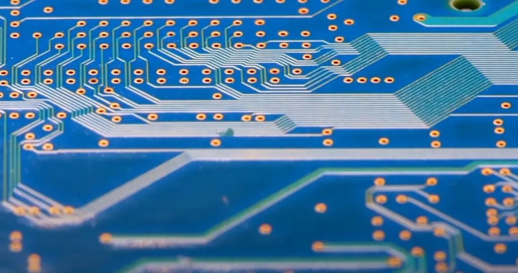
You should use vias in a printed circuit board (PCB) design whenever you need to connect signal traces between layers, or when you need to make power and ground connections. Vias can also be used to increase trace density, reduce the size of the PCB, and improve thermal management.
The use of vias in a PCB design is essential when designing high-speed circuits. Vias help to reduce electromagnetic interference (EMI) and improve signal integrity and are particularly useful for differential signal transmission, which is necessary for high-speed data transmission applications.
In addition to signal routing and power connections, vias can also be used for thermal management on a PCB. By routing copper layers between vias, heat generated by components on the PCB can be dissipated more effectively.
How Do I Use Blind And Buried Vias in My Design?
Using blind and buried vias in your PCB design can help you save space and reduce signal interference.
Here are some steps you can follow to use blind and buried vias in your design:
- Determine the layers that need to be connected: Identify the layers that need to be connected using blind or buried vias. This will depend on the specific requirements of your design;
- Choose the appropriate via type: Select the appropriate via type based on the layers that need to be connected. Blind vias connect an outer layer to an inner layer, while buried vias connect inner layers only;
- Determine the via size: Determine the appropriate via size based on the current-carrying capacity and the amount of heat generated by the current. Use manufacturer guidelines and software tools to determine the appropriate size;
- Place the vias: Place the vias in your design using your PCB design software. Ensure that they are placed in the correct locations and that they do not interfere with other components or traces;
- Check for design rule violations: Run a design rule check to ensure that your design complies with the manufacturing guidelines and requirements;
- Generate Gerber files: Generate Gerber files for the PCB manufacturer, which will include the specifications for the blind and buried vias;
- Verify manufacturing capabilities: Verify that the manufacturer has the capability to manufacture blind and buried vias according to your design specifications [8];
What Size Should Vias Be?
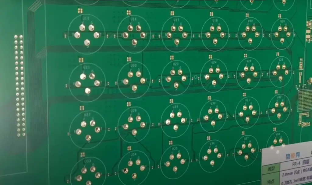
The size of vias can vary depending on the specific application and the requirements of the circuit board. However, in general, the size of vias is typically determined by the smallest drill size that can be used in the PCB manufacturing process.
The minimum via size is typically determined by the manufacturer’s capabilities and the design rules for the specific PCB manufacturing process being used. As a rule of thumb, the minimum diameter of a via should be at least 0.3 mm for most PCB manufacturing processes.
However, the size of vias can also be influenced by other factors such as the current carrying capacity of the via, the thermal conductivity required for the application, and the space available on the board. Therefore, it is important to carefully consider the specific requirements of the circuit board and consult with the PCB manufacturer to determine the appropriate size for the vias.
Considerations For Creating Vias:
- Via type. There are three main types of vias – through-hole vias, blind vias, and buried vias. Through-hole vias extend completely through the PCB, while blind vias only connect the top and bottom layers of the PCB, and buried vias connect the internal layers of the PCB. The type of via you choose will depend on your specific design requirements;
- Via size. The size of the via should be selected based on the size of the trace, the current carrying capacity, and the requirements of the intended operating environment. If the current required to be carried is high or the operating environment experiences high vibration, for example, a larger via size may be necessary to ensure mechanical stability;
- Location. Vias should be placed carefully to avoid interference with other traces or components on the PCB. Consideration should be given to the signal routing path, the number and density of components, and any other potential sources of interference;
- Routing. The routing of traces connected to the via should be carefully planned to ensure adequate clearance and avoid interference. For high-speed signals, spacing and impedance control should be considered to ensure signal integrity;
- Manufacturing considerations. The specific type of via to be used should be selected based on the capabilities of the manufacturer being used, and whether the PCB is a single or double sided board. Depending on the type of via used, additional manufacturing steps may be required [9];
FAQ
1. Should you avoid vias in PCB design?
No, vias are an important part of PCB design and are commonly used to route signals between layers, increase routing density, and improve signal integrity. However, it is important to carefully consider the placement and size of vias in order to avoid potential manufacturing issues or signal integrity problems.
2. What do vias mean in electronics?
In electronics, vias refer to small holes drilled into a PCB that is filled with a conductive material, allowing for electrical connections between layers of the PCB.
3. Do vias make PCBs more expensive?
Vias themselves do not necessarily make PCBs more expensive. However, the cost of adding vias to a PCB design may increase if special manufacturing processes or materials are required.
4. Do vias increase the cost of a PCB?
Yes, vias can increase the cost of a PCB. Vias require additional processing steps during manufacturing and drilling, which adds to the production cost. The cost also depends on the number of vias, their size, and the complexity of the design.
5. Do vias connect all layers?
Not necessarily. Vias can be designed to connect only a few specific layers of a PCB. Some vias, such as through-hole vias, connect all layers of a PCB, while others, such as blind and buried vias, connect only a limited number of layers.
6. What is the difference between trace and via in PCB?
A trace in a PCB refers to a conductive path on the surface of the board that carries electrical signals between components. A via, on the other hand, is a hole in the PCB that connects different layers of the board, allowing signals to pass through.
7. What is the difference between plugged and tented vias?
A plugged via is one that has been filled with a conductive or non-conductive material, whereas a tented via is one that has been covered with a solder mask or other material to prevent the solder from entering the hole.
8. What is a blind via in PCB?
Blind vias are used to save space and reduce the number of layers in a PCB.
9. How do you test for PCB via?
The most common method to test for PCB via is to use a continuity tester, such as a multimeter. By connecting the probes to each side of the via, the continuity can be checked to ensure that the via is functioning properly.
10. Do vias need to be filled?
Not all vias need to be filled, but it depends on the specific design requirements. Some designs may require the via to be filled with a conductive or non-conductive material to enhance electrical performance or to prevent solder from entering the via.
11. What is the difference between stacked and blind vias?
Stacked vias are multiple vias that are drilled on top of each other, while blind vias are vias that connect an outer layer of a PCB to an inner layer without passing through the entire board. Stacked vias are used to save space and reduce the number of layers in a PCB, while blind vias are used to reduce the size of the PCB.
12. How much distance is between two vias?
The distance between two vias depends on the specific design requirements and the size of the vias. In general, it is recommended to keep a distance of at least 3 times the diameter of the via between two vias.
13. What is the difference between vias and pads?
Vias are used to connect different layers of a PCB, while pads are used to provide a connection point for a component or a trace on the same layer of the PCB.
14. Do PCBs break down easily?
PCBs can break down if they are subjected to excessive heat, moisture, or mechanical stress. However, if they are designed and manufactured properly, they can be very reliable and have a long lifespan.
15. What are vias in double-sided PCB?
In a double-sided PCB, vias are used to connect the traces on one side of the board to the traces on the other side of the board [10].
16. What are the advantages of buried vias?
Buried vias provide a way to connect multiple layers of a PCB without increasing the board thickness or size. This allows for more efficient use of space and can reduce the overall cost of the board.
17. Are PCBs safe to touch?
PCBs are generally safe to touch, but it depends on the specific application and the materials used in the PCB. Some PCBs may contain hazardous materials such as lead or other heavy metals, which can be harmful if ingested or inhaled. It is important to follow proper handling and disposal procedures for PCBs to ensure safety.
18. What material is used for vias?
The most common material used for vias is copper, which is a good conductor of electricity and is easy to work with during the manufacturing process. Other materials such as gold, silver, or aluminum may also be used depending on the specific application.
19. What thickness are vias?
The thickness of a via depends on the diameter of the hole and the number of layers it is connecting. In general, the thickness of a via ranges from 0.1mm to 0.3mm [11].
20. Do vias connect all layers?
Not necessarily. Vias can be designed to connect only a few specific layers of a PCB. Some vias, such as through-hole vias, connect all layers of a PCB, while others, such as blind and buried vias, connect only a limited number of layers.
21. What is the hole tolerance for PCB via?
The hole tolerance for a PCB via depends on the specific manufacturing process and design requirements. In general, the hole tolerance ranges from +/- 0.05mm to +/- 0.1mm [12].
22. What is the IPC standard for vias?
The IPC standard for vias is IPC-A-600, which provides guidelines for the acceptance criteria for the quality of printed circuit boards.
23. How do you calculate via size in PCB?
The via size in a PCB is calculated based on the current-carrying capacity and the amount of heat generated by the current. The size of the via is also determined by the pitch of the components and the routing density of the board. The design engineer can use software tools and manufacturer guidelines to determine the appropriate via size for a specific design.
Useful Video: What is a PCB Via?
References
- https://www.proto-electronics.com/blog/how-and-where-use-vias-in-pcb-design
- https://resources.pcb.cadence.com/blog/2020-vias-types-and-applications
- https://en.wikipedia.org/wiki/Via_(electronics)
- https://www.ourpcb.com/pcb-via.html
- https://www.allaboutcircuits.com/technical-articles/which-via-should-i-choose-a-guide-to-vias-in-pcb-design/
- https://www.wevolver.com/article/what-is-a-via-a-comprehensive-guide
- https://www.raypcb.com/via-in-pcb/
- https://www.pcbdirectory.com/community/what-is-a-via
- https://www.eurocircuits.com/via-via-hole/
- https://www.protoexpress.com/kb/pcb-via-design/
- https://www.ncbi.nlm.nih.gov/pmc/articles/PMC7330927/
- https://www.mclpcb.com/blog/guide-to-pcb-grounding-techniques/











Leave a Reply